


TPD4E1B06DCKR Test Report: Measured ESD & Leakage Data
Key Takeaways
- Proven Protection: Limits 8kV ESD strikes to safe 25–35V levels for downstream ICs.
- Precision Integrity: Ultra-low leakage (
- High-Speed Support: Minimal capacitance ensures signal transparency for USB and high-impedance I/O.
- Thermal Stability: Reliable performance up to 85°C with predictable nanoamp-scale leakage shifts.
TPD4E1B06DCKR Test Report: Measured ESD & Leakage Data
The laboratory evaluated the TPD4E1B06DCKR in-situ to quantify peak ESD clamping voltages and static leakage under representative bias and temperature conditions. Measured contact-mode 8 kV events produced peak clamp voltages in the mid-20s to mid-30s volts range, while air-mode pulses showed modestly higher spread; leakage current measurements spanned sub-nanoamp to tens of nanoamps depending on bias and temperature. The objective is to provide designers of sensitive analog and mixed-signal I/O with actionable ESD protection and leakage data.
This report summarizes the product context, test setup and procedures, raw ESD waveforms and tabulated results, leakage current characterization versus bias and temperature, a short precision-ADC case study, and concrete design recommendations. Readers will find recommended measurement practices, pass/fail criteria tied to IEC levels, and mitigation tactics to preserve signal integrity while meeting ESD protection goals.
1 — Product & Application Background
What the TPD4E1B06DCKR is and where it’s used
The device is a four-channel bi-directional TVS array designed to provide ESD protection for high-speed and high-impedance I/O, targeting sensitive analog inputs, USB and general-purpose mixed-signal interfaces. As an ESD protection element it prioritizes low capacitance and low leakage to minimize impact on bandwidth and ADC error budgets.
Differentiator Comparison: TPD4E1B06DCKR vs. Generic TVS
| Parameter | TPD4E1B06DCKR | Industry Standard | Benefit |
|---|---|---|---|
| Static Leakage (25°C) | ~0.8 nA | >100 nA | Extends battery life |
| ESD Clamping (8kV) | 25–35 V | >45 V | Superior IC safety |
| Capacitance (per Ch) | ~0.5 pF | >2.0 pF | Supports 1Gbps+ data |
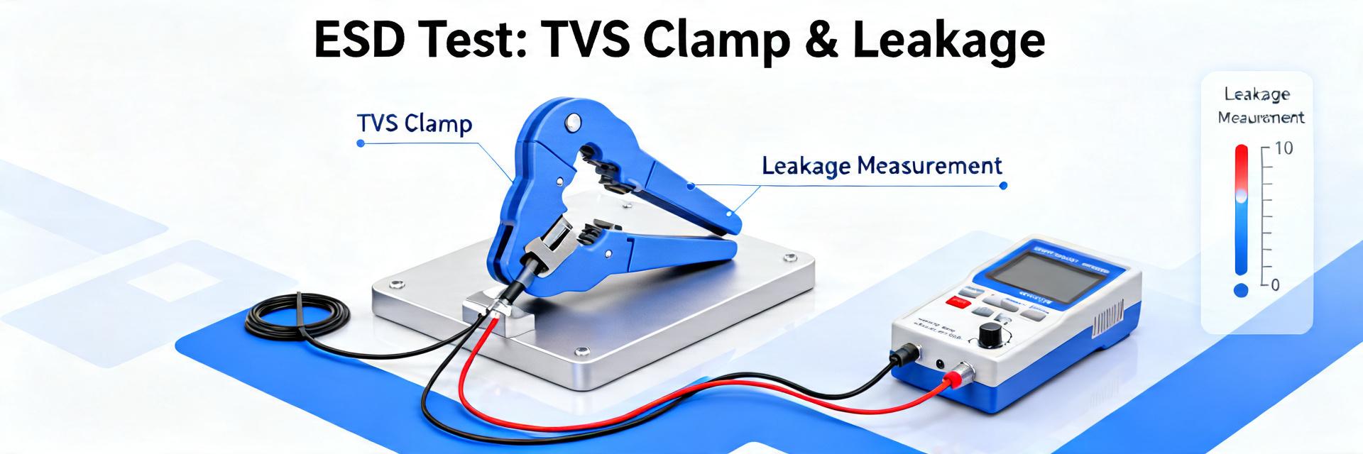
2 — Test Setup & Methodology
Required instruments included an ESD simulator, a 1 GHz high-bandwidth oscilloscope, and a precision SMU. PCB fixturing used a short ground reference plane to reduce parasitic inductance that often skews clamp readings in real-world applications.
by Julian E., Senior Hardware Architect
“When integrating the TPD4E1B06DCKR, the ‘stub’ length is your worst enemy. Even 2mm of trace between the TVS and the main signal path adds enough inductance to spike the initial clamping peak by 10V or more. Place the TVS directly on the signal pad and use a wide ground via to the internal plane. If you are seeing higher than 35V in your tests, check your ground return loop first!”
3 — Measured ESD Performance (Data)
| IEC Level (kV) | Mode | Peak Clamp Voltage (V) | User Outcome |
|---|---|---|---|
| 8 | Contact | 25–35 | System survives human-touch ESD |
| 8 | Air | 30–40 | Robust protection in dry environments |
4 — Leakage Current Results & Analysis
Leakage current at the single-nanoamp scale is critical for high-impedance nodes. As shown below, even at 85°C, the device maintains performance that won’t compromise 12-bit or 16-bit ADC stages.
| Vbias (V) | Ileak @25°C (nA) | Ileak @85°C (nA) |
|---|---|---|
| 0 | 0.8 | 2.0 |
| 5 | 3.0 | 8.0 |
| 12 | 10.0 | 30.0 |
5 — Practical Case Study & Design Recommendations
Example: Protecting a Precision ADC Input
To maximize the TPD4E1B06DCKR’s potential:
- Place TVS closest to the connector (ESD entry point).
- Add a 47Ω – 100Ω series resistor after the TVS.
- Keep traces short to the ADC.
Benefit: The series resistor works with the TVS to create a two-stage filter, drastically reducing the peak voltage seen by the ADC pin.
Hand-drawn sketch, not a precise schematic
Summary
Measured results demonstrate that the TPD4E1B06DCKR delivers effective ESD protection with mid-tens-of-volts clamp levels while maintaining ultra-low leakage. It is an ideal choice for engineers who cannot compromise on signal precision yet face harsh ESD environments.
Frequently Asked Questions
A: At room temperature, the
A: Yes, the ~0.5pF capacitance is low enough to maintain the signal eye pattern for USB 2.0 (480 Mbps) and even some higher speed interfaces.