


SN65LBC184DR RS-485 Datasheet Deep Dive: Key Specs
SN65LBC184DR RS-485 Datasheet Deep Dive: Key Specs
In bench validation and datasheet summaries, the SN65LBC184DR shows protection and differential-transceiver characteristics that map directly to board-level design choices. This deep dive decodes the Datasheet to highlight the electrical and robustness specs that determine cable length, data rate, and margin decisions for noisy industrial RS-485 links. The goal is practical guidance: what to read, what to test, and how to implement reliably.
Readers will find device role and topology context, prioritized driver and receiver parameters, protection and thermal considerations, PCB and termination best practices, and a concise test checklist. Each section focuses on action: extract the right numbers from the Datasheet, translate them into layout and test choices, and verify behavior on the bench before field deployment.
Background & device overview (background introduction type)
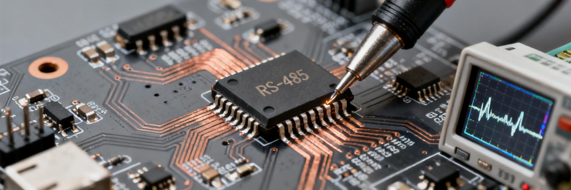
What the SN65LBC184DR is — role and block-level description
Point: The SN65LBC184DR is a half-duplex differential transceiver combining one driver and one receiver in a single package for single-ended system interfacing. Evidence: The block-level design pairs a differential driver with a fail-safe receiver and VCC decoupling pin nearby. Explanation: In practice this means one IC can both drive and listen on a two-wire RS-485 bus, simplifying multi-drop and point-to-point topologies while reducing board area and BOM.
Standards, compatibility, and common application domains
Point: The device targets RS-485 networks while offering compatibility with related balanced interfaces. Evidence: Key features include wide common-mode tolerance and fail-safe behavior to support multi-drop buses. Explanation: Typical uses are industrial automation, building control, and serial links where robustness and low-power operation are priorities; the part is selected when a compact, protected half-duplex transceiver is required.
Electrical characteristics — driver & receiver key specs (data analysis type)
Driver electrical specs to prioritize
Point: Extract supply range, differential output capability, short-circuit limits, data-rate/slew characteristics, and propagation delays from the Datasheet. Evidence: Supply range bounds system-level decoupling and logic compatibility; VO(min/max) and driver short-circuit current determine safe cable loading and fault behavior. Explanation: Use VO and short-circuit numbers to compute worst-case bus voltages and dissipation; pair propagation delay and slew-rate limits with bus length to estimate maximum reliable baud rate and eye margin.
| Parameter | Why it matters | Design action |
|---|---|---|
| Supply voltage range | Defines VCC tolerance and decoupling needs | Place 0.1µF + 1µF caps close to VCC pin |
| Differential output amplitude | Affects cable reach and receiver margin | Model worst-case load (e.g., 54Ω) to predict VO |
| Slew rate / data-rate | Limits max baud and EMI | Use external slew control or lower baud for long runs |
Receiver performance and input tolerances
Point: Focus on input sensitivity, valid differential thresholds, common-mode range, hysteresis, and fail-safe thresholds. Evidence: These specs determine whether the receiver sees valid logic amid cable-induced offsets and ground shifts. Explanation: A wide common-mode range and robust fail-safe mean fewer false transitions with floating or biased buses; ensure bias networks and termination maintain differential idle voltages inside the receiver’s thresholds for reliable idle-state detection.
Robustness & protection features (data/method combined)
Transient protection and ESD ratings
Point: Evaluate ESD and transient specs to judge field survivability. Evidence: The Datasheet lists ESD contact/air discharge levels and transient suppression behavior; these ratings predict susceptibility to cable discharge and surge events. Explanation: On the bench, validate claims with contact-discharge checks, controlled surge injections across the pair, and observing clamping behavior; pair on-chip protection with external TVS parts sized for expected surge energy on long cable runs.
Thermal limits, power dissipation, and reliability margins
Point: Use junction-to-ambient thermal resistance, maximum junction temperature, and power dissipation to compute derating. Evidence: The Datasheet provides θJA and absolute maximum temperatures that set permissible continuous dissipation. Explanation: Calculate expected power from driver active duty cycle and load; ensure PCB copper area and thermal vias keep ΔT acceptable, and add derating margin for elevated ambient in enclosures.
Implementation best practices — PCB, termination & biasing
PCB layout and grounding recommendations
Point: Layout dictates EMI, common-mode coupling, and thermal behavior. Evidence: Best practice places decoupling close to VCC, minimizes stub lengths on the differential pair, and separates analog/digital grounds where necessary. Explanation: Route the pair together with controlled impedance, keep them away from switching supplies, place bypass caps within 1–2mm of VCC, and locate TVS devices at cable entry to avoid routing transient energy through sensitive traces.
Bus termination, bias networks and protection components
Point: Proper termination and biasing preserve signal integrity and idle states. Evidence: Use matched termination (typically 120 Ω across the pair) and a bias network to hold idle differential above receiver thresholds. Explanation: For half-duplex lines, place termination at ends only; bias with resistor divider values chosen to source/sink minimal current while holding the bus in the receiver’s fail-safe range. Add series fusing or polyfuse for surge protection on exposed networks.
Testing, troubleshooting & performance checklist
Bench and field test checklist
Point: A repeatable test sequence verifies functionality and robustness. Evidence: Start with DC continuity and isolation, then measure quiescent current at power-up, capture driver differential waveform under load, evaluate common-mode tolerance with applied offset, and run BER tests at target baud. Explanation: Use differential probes and a scope with ≥200MHz bandwidth, set proper probe grounding, and log results; include quick ESD discharges and observe clamping to verify protection.
Common failure modes and fixes
Point: Many field faults are configuration or layout related. Evidence: Typical symptoms include reflections from missing termination, inverted polarity, and bus locking due to failed bias. Explanation: Diagnose with scope captures: missing termination shows overshoot and ringing, swapped A/B yields inverted logic, thermal issues show elevated VCC or thermal shutdown. Remedies: add correct termination, correct pinout, strengthen bias network, and improve thermal dissipation.
Summary
- The SN65LBC184DR is a compact half-duplex RS-485 transceiver; prioritize proper termination, biasing, and protection to translate Datasheet specs into reliable field behavior.
- Key electrical limits (driver VO, short-circuit current, receiver common-mode range) set cable length and data-rate choices; validate on the bench with differential scope captures.
- Combine on-chip protection with external TVS and careful PCB thermal planning to maximize uptime in industrial deployments.
FAQ
What are the essential SN65LBC184DR Datasheet numbers to check before layout?
Answer: Prioritize supply range, differential output amplitude under specified load, propagation delay and slew limits, receiver input threshold and common-mode range, and thermal θJA. These determine decoupling, termination resistor choice, estimated max baud for a given cable length, and required PCB copper for thermal dissipation. Verify each with a short bench validation sequence.
How should I bias and terminate an RS-485 bus when using SN65LBC184DR?
Answer: Use 120 Ω termination at the physical ends of the bus and a bias network that holds the idle differential voltage inside the receiver’s fail-safe window—typically a pair of resistors and a pull resistor to VCC or GND creating a small offset. For half-duplex, place termination only at ends and ensure bias source is stronger than leakage currents from nodes.
Which bench tests confirm RS-485 robustness for the SN65LBC184DR?
Answer: Perform DC continuity and isolation checks, measure quiescent currents, capture differential driver waveforms into the worst-case load, apply known common-mode offsets, and run BER tests at the target baud. Also execute controlled ESD/contact checks and observe TVS clamping to confirm transient behavior under realistic cable conditions.