


SI1308EDL-T1-GE3: Compact MOSFET Specs & Rds(on) Data
The SI1308EDL-T1-GE3 is presented in the manufacturer datasheet as a compact 30 V N‑channel MOSFET with an Rds(on) reported near 132 mΩ at a 10 V gate drive; this single data point makes it attractive for space‑constrained low‑voltage switching and load‑switch roles. Designers should treat that figure as a baseline, verifying under their own gate drive and temperature conditions to avoid underestimating conduction losses.
This article breaks down datasheet numbers, shows how Rds(on) varies with VGS and Tj, outlines practical bench methods and loss calculations, and gives layout and selection tips for US hardware engineers.
SI1308EDL-T1-GE3 — at-a-glance specs and package
Quick-spec snapshot
| Parameter | Typical / Nominal | Test Condition |
|---|---|---|
| Vdss | 30 V | DC |
| Continuous drain current | ~1.4–1.5 A | Ta/Tc rated |
| Rds(on) | ~132 mΩ | VGS = 10 V, 25°C |
| VGS|max | ±12 V (typical) | Absolute Limit |
| VGS(th) | Gate Threshold | Id test condition |
| Ciss / Crss | Low Capacitance | For switching efficiency |
| ESD rating | Internal Protection | See datasheet Class |
| Power dissipation | Package Dependent | Thermal relief required |
Package, footprint and thermal limits
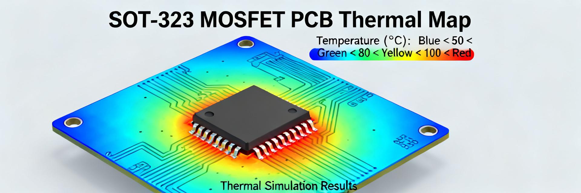
The device is housed in a compact SOT‑style package with limited thermal mass. Practitioners should allocate copper pour and vias under the package, follow the recommended footprint, and note that small packages require conservative continuous current assumptions unless substantial PCB thermal relief is provided.
SI1308EDL-T1-GE3 Rds(on) behavior: test conditions & temp effects
How datasheet Rds(on) is measured
Datasheet Rds(on) numbers are measured under specific, sometimes pulsed, conditions. A typical measurement uses VGS = 10 V and a defined Id or pulse to limit self‑heating, often referenced at 25°C. Designers must check whether the quoted Rds(on) is pulsed or DC; using a pulsed number for continuous thermal environments will understate losses.
Temperature coefficient and real-world implications
Rds(on) rises with junction temperature, increasing conduction loss. Conduction loss Pcond = I² × Rds(on); for example, at I=1 A and Rds(on)=132 mΩ, Pcond≈0.132 W. If Rds(on) increases 50% at elevated Tj, Pcond becomes ≈0.198 W. Include derating margins and thermal modeling when designing for continuous currents.
Data deep-dive: bench measurements and characteristic curves
Recommended measurement setup and method
Accurate Rds(on) measurement requires Kelvin sense and short pulses to avoid self‑heating. Best practice uses <1 ms pulses and calibrated current sense with low burden. Avoid long leads and poor contact resistance; record VGS, Id, and temperature, repeating at logic‑level gate voltages if used in the application.
Interpreting curves
Transfer (Id vs VGS) and output curves drive selection beyond Rds(on). Gate charge (Qg) and capacitances determine driver power and switching losses at frequency. Extract Qg and compute Pgate = Qg × Vdrive × fSW for gate driver sizing.
Application examples — where the MOSFET fits best
- Low-voltage load-switch: Ideal for battery-powered roles under 1–2 A where conduction loss remains modest.
- DC-DC Converters: Suitable for low-current converters; however, at high fSW, gate charge and Coss become the dominant loss factors.
Practical selection checklist & PCB/layout tips
Choose this device when space is constrained and gate drive can deliver 10 V. For layout, use short source traces for Kelvin sense, place decouplers close to drain/source, and use 5–47 Ω gate resistors to reduce ringing. Add copper pour and thermal vias to spread heat effectively.
Key summary
- Baseline: Compact 30 V N‑channel MOSFET, Rds(on) ≈132 mΩ @ VGS=10 V.
- Verification: Always verify Rds(on) under intended junction temperature; pulsed specs differ from DC continuous values.
- Layout: Thermal vias and copper pours are critical for continuous current capability.
Common questions
What is the Rds(on) of SI1308EDL-T1-GE3 at 10 V?
How to measure Rds(on) without self-heating?
Is this MOSFET suitable for 1 A continuous switching?
What is the primary application for this MOSFET?
For further reading, see internal resources:
MOSFET measurement best practices,
Power loss calculation guide, and
PCB thermal vias and copper plane design.