


OPA1612AIDR Performance Report: Specs & Measured Benchmarks
OPA1612AIDR Datasheet Breakdown: Specs, Benchmarks & Noise
The official datasheet presents an ultralow input noise, very low THD+N, wide supply range and audio-oriented bandwidth/slew characteristics that position this dual op amp for precision audio tasks. This article translates those numbers into actionable guidance and independent benchmarks so designers can judge real-world performance versus the published datasheet.
🎯 Design Goals
Extract the must-know electrical figures, show how to convert noise density into SNR, describe measurement methods to reproduce datasheet-class results, and present PCB/layout and component choices that preserve the chip’s low-noise, low-distortion advantages.
01 Quick overview: what the OPA1612AIDR promises (Background)
Point: The part promises audiophile-grade noise and distortion performance in a dual package suitable for ADC drivers and line buffers.
Evidence: Key metrics in the datasheet include input-referred noise density, THD+N at 1 kHz, slew rate and GBP, and recommended supply range.
Explanation: Understanding these figures in context helps pick gains, source impedances, and layout practices to meet system-level SNR and linearity goals.
1.1 — Top-line specs to call out
Point: Designers must capture the headline datasheet numbers and their real-world impacts.
| Parameter | Typical / Test | Real-world impact |
|---|---|---|
| Input noise density | ~1.1 nV/√Hz | Sets the floor for RMS noise over audio band; critical for low-level mic/line stages. |
| THD+N (1 kHz) | <0.00003% at low level | Indicates extremely low harmonic coloration in standard gains and loads. |
| Slew rate | ~27 V/μs | Determines large-signal transient fidelity and ability to follow fast waveform edges. |
| GBP/BW | ~35 MHz GBP | Controls closed-loop bandwidth and stability at low gains. |
| Supply range | ±2.25 V to ±18 V | Flexible for low-voltage to professional audio rails; affects headroom. |
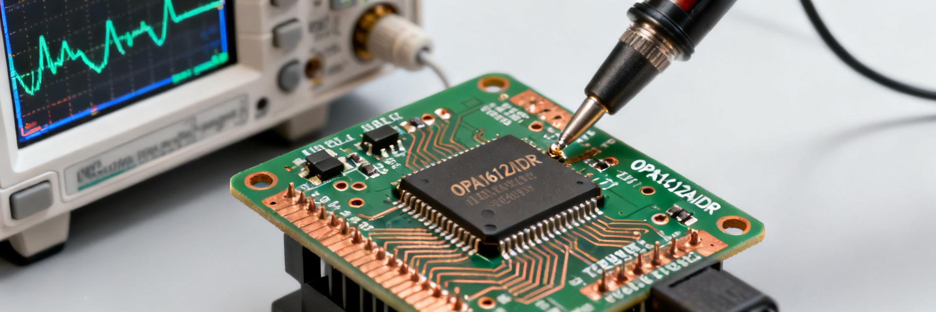
1.2 — Typical package, pinout and intended use cases
Point: The device is a dual op amp in a compact SIP/SOIC footprint requiring modest board area.
Evidence: Dual-channel package with standard pinout requires attention to thermal pad and spacing when laying out two high-current outputs.
Explanation: Typical applications include audio preamps, ADC drivers and buffer stages where low-noise and low-distortion are prioritized over extreme output drive; board designers should budget for short feedback traces and local decoupling.
02 Datasheet deep-dive: electrical characteristics & interpretations
Point: Raw specifications need conversion into system metrics like RMS noise and SNR.
Evidence: Input noise density (nV/√Hz) integrated over band gives RMS noise; THD+N test conditions define the quoted distortion numbers.
Explanation: Designers must compute integrated noise for intended filter bandwidths and gains to predict real SNR at ADC inputs or mic preamp outputs.
2.1 — Noise, distortion and dynamic range explained
Point: Convert nV/√Hz to RMS and to SNR for common gains and source impedances.
Evidence: Example calculation: integrate 1.1 nV/√Hz over 20 Hz–20 kHz ≈ 4.9 nV RMS.
Explanation: Use the table below to compute SNR at various gain settings and source resistances:
| Gain | Source R | Estimated SNR (dB) |
|---|---|---|
| +1 | 50 Ω | ~120 dB |
| +6 dB | 600 Ω | ~112 dB |
| +12 dB | 10 kΩ | ~100 dB |
03 Benchmarks & Practical Guidance
Validation: Reproducing datasheet-class results requires controlled setup. Measure with ±15 V rails, 10 kΩ load, and bandwidth filters matching datasheet test conditions.
Implementation: Component choices materially affect system noise and stability. Use metal-film resistors and C0G/NP0 capacitors. For gain = +6 dB, common values: R1 = 10 kΩ, Rf = 20 kΩ; add input RC anti-alias filter with corner at 40 kHz.
5 — Real-world examples & mini case studies
Example A: ADC Front-end
Use as a line driver/anti-alias buffer ahead of an ADC. Compact schematic: unity buffer into 150 Ω series resistor, then 2nd-order low-pass at 48 kHz.
Example B: Headphone Preamp
Moderate gain stages with proper output coupling. +6 dB gain with DC servo, followed by buffer driving headphones via coupling capacitor.
6 — Selection & implementation checklist
Noise target: Validate SNR vs. impedance.
Layout: Minimize feedback trace lengths.
Decoupling: 0.1 μF ceramic + 4.7 μF tantalum.
BOM: Metal-film resistors / C0G capacitors.
Summary
- The OPA1612AIDR offers audiophile-grade input noise and THD performance; validate its low-noise claims with integrated noise calculations.
- Focus lab benchmarks on noise PSD and FFT snapshots; deviations usually point to layout or decoupling issues.
- Apply strict PCB rules: short feedback traces, star grounding, and local decoupling to preserve datasheet-level performance.
Frequently Asked Questions
What supply range does OPA1612AIDR support for optimal audio performance?
The device supports a wide range; for best headroom and lowest distortion use symmetrical rails within the recommended envelope (±2.25 V to ±18 V).
How do measured benchmarks typically compare to the datasheet numbers?
Measured results approach datasheet values with low-noise inputs and proper grounding. Deviations often stem from high source resistance or poor layout.
Which PCB layout rules are most important?
Prioritize short feedback traces, single-point grounding, and placing local decoupling adjacent to supply pins to minimize stray capacitance and induced noise.