


MWSA0603S-R47MT in High-Current Designs: Real Layout Tips
MWSA0603S-R47MT PCB footprint & assembly guide for SMD
• High-Current SMD Inductors
Use the recommendations below as a starting point, validate with first-article inspection and iterate paste coverage and pad fillet expectations based on measured results. The guidance combines datasheet-driven constraints, PCB layout best practices, and assembly-level controls to reduce common failure modes.
1
Quick component overview & why footprint matters
1.1 Component role & electrical/mechanical summary
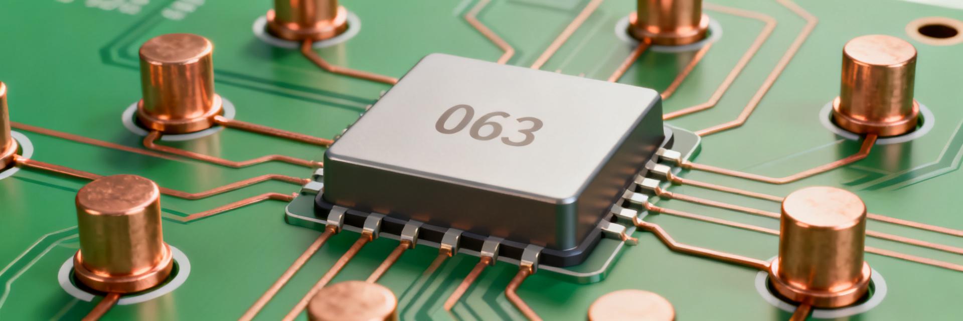
Point: The MWSA0603S-R47MT is a molded, high-current power inductor in an 0603-class package used for DC‑DC converters and power filtering.
Evidence: typical specs to check are rated current (saturation and thermal), DCR, inductance (0.47 µH nominal), and package height and terminations.
Explanation: those electrical and mechanical parameters directly drive pad area, copper pour, and clearance decisions because current density, heating and mechanical support must be balanced to preserve performance and reliability.
1.2 Failure modes linked to wrong footprints
Point: Specific footprint mistakes map to predictable failures.
Evidence: insufficient pad length or asymmetric paste coverage leads to tombstoning; undersized copper causes thermal derating and elevated DCR; tight clearance to other components increases magnetic coupling and EMI.
Explanation: identify each failure mode (tombstone, cold joint, overheating, mechanical lift) and correct by adjusting pad geometry, paste percentage and copper thermal relief based on the component’s electrical/thermal demands.
2
Datasheet & measurement-driven constraints
2.1 Key mechanical dimensions
Point: Extract and prioritize body length/width/height, termination geometry and any recommended land pattern.
Evidence: datasheet tolerances on termination width and edge radii determine minimum pad overlap and solder fillet expectations.
Explanation: use the largest termination tolerance when sizing pads to ensure reliable solder fillets; account for height variation in pick-and-place z-limits and stencil stepping to avoid solder starvation or excessive squeeze-out.
2.2 Electrical and thermal constraints
Point: Current handling and thermal derating define copper and via strategy.
Evidence: rated current and DCR point to necessary trace width, plane area and thermal vias to maintain acceptable temperature rise.
Explanation: when the inductor is a primary current path, specify heavy copper or stitched plane under the pad, add vias for heat spreading, and derate current by 10–30% in early prototypes; document thermal relief exceptions for assembler use.
3
Recommended PCB footprint & land pattern
3.1 Exact pad geometry & dimensions
A balanced land pattern gives reliable fillets and mechanical support while minimizing tombstoning. Include 0.05 mm soldermask expansion and a nominal 0.1 mm paste mask reduction per pad to control paste volume.
3.2 Stencil & solder paste recommendations
Controlled paste volume prevents tombstoning and under/over-soldering. Start with 60–70% paste coverage per termination using rectangular apertures aligned to the pad, and a 0.1 mm step‑down from pad outline for aperture length and width. Use a 0.12–0.15 mm stainless stencil thickness as baseline for 0603 power devices.
4
Pick-and-place, reflow, and assembly
4.1 Pick-and-Place
Consistent orientation and nozzle matching reduce misplacement and rotation. Place the inductor long axis parallel to the X or Y fiducial grid, use a small open-cone or 0603‑capable nozzle with suction equalization, and limit placement speed to maintain ±0.1 mm accuracy.
4.2 Reflow Profile
A controlled reflow ramp and peak protects part integrity while achieving proper wetting. Use a lead‑free profile with preheat to 150–180°C (60–90 s soak), ramp 1–3°C/s to peak 235–245°C, and cool at ≤4°C/s. Validate joints visually and with X‑ray for hidden fillets.
5
PCB layout examples & common mistakes
5.1 Layout Do’s
- Place close to switching nodes (2-5mm)
- Use generous copper for traces
- Stitch plane vias on pad perimeter
- Add keep-out zones for sensitive circuits
5.2 Top 6 Mistakes
- Pads too small (Enlarge 10-20%)
- Excessive paste coverage
- Silkscreen over pads
- Insufficient copper/thermal relief
6
Manufacturing checklist
6.1 Files and documentation
Supply Gerber, paste and mask files, pick-and-place centroid with rotation, BOM with exact footprint reference, and assembly notes indicating paste percent. Clear handoff prevents misinterpretation and allows the assembler to replicate prototype settings.
6.2 Final QA tests and FAI
Perform visual and X‑ray sampling (10% of assemblies), functional test under nominal load, and a short thermal soak. Set pass thresholds for wetting and temperature rise to reveal thermal derating early.
Frequently Asked Questions
What PCB footprint tolerances should I use for MWSA0603S-R47MT?
Use pad dimensions sized to the maximum termination tolerance: nominally 0.9 mm × 0.6 mm pads with ±0.05 mm placement tolerance. Include 0.05 mm soldermask expansion and a 0.1 mm paste reduction.
How do I prevent tombstoning during assembly of this high-current SMD inductor?
Balance paste volume between the two terminations (60–70%) and use a 0.12–0.15 mm stencil. Ensure symmetric pad shapes and controlled ramp-to-peak reflow (1–3°C/s).
What inspection criteria confirm an acceptable solder joint for power inductors?
Acceptable joints show continuous wetting, fillet covering ≥50% of the termination edge, and no bridges. X‑ray voids should be under 20% of pad area.