


MAX9244EUM+TD Datasheet Deep Dive: Key Specs & Limits
Key Takeaways (GEO Summary)
- High-Speed Throughput: Achieves 306 Mbps per link, enabling real-time HD sensor data transmission.
- Industrial Reliability: Robust -40°C to +85°C range with ±30kV ESD protection for harsh environments.
- Optimized Integration: 21-bit deserialization translates to 20% less PCB complexity compared to discrete solutions.
- LVDS to LVCMOS: Seamlessly bridges high-speed differential signals to standard digital backends.
MAX9244EUM+TD Datasheet Deep Dive: Key Specs & Limits
The MAX9244EUM+TD datasheet frames this 21‑bit deserializer as a high‑density LVDS receiver with LVCMOS/LVTTL outputs, a per‑link rate near 306 Mbps, a 3.0–3.6 V supply window, and an operating range of −40 °C to +85 °C. These headline numbers establish the safe operating envelope; this deep dive will translate those datasheet entries into actionable electrical limits, concrete test steps, and design rules engineers can use during validation and system bring‑up.
Competitive Comparison: MAX9244 vs. Industry Standards
| Feature | MAX9244EUM+TD | Generic 18-bit SerDes | User Benefit |
|---|---|---|---|
| Data Resolution | 21-Bit | 18-Bit | 16% higher data density per clock |
| ESD Protection | ±30kV (Air) | ±8kV to ±15kV | Eliminates external TVS in many cases |
| Throughput | 306 Mbps/lane | ~200 Mbps/lane | Supports higher resolution/frame rates |
1 — Product overview & datasheet essentials (background introduction)
1.1 What the device is and where it fits
Point: The device is a 21‑bit deserializer intended for short‑reach camera and sensor interfaces. Evidence: The official manufacturer datasheet describes LVDS differential inputs feeding single‑ended LVCMOS/LVTTL outputs and a multi‑lane deserializer topology. Explanation: In practice this places the part in camera links, automotive sensor bridges, and multi‑sensor aggregators where compact LVDS links feed a digital backend at roughly 300 Mbps per lane.
1.2 Quick reference: headline specs table
| Parameter | Value | Note |
|---|---|---|
| Data rate | ~306 Mbps per link | Recommended operating |
| Resolution / bits | 21 bits | Functional |
| Input / Output types | LVDS inputs / LVCMOS & LVTTL outputs | Signal I/O |
| Supply rails | 3.0 – 3.6 V | Recommended (abs max higher) |
| Operating temp | −40 to +85 °C | Recommended |
| ESD | ±30 kV (air), ±6 kV (contact) | Absolute test ratings |
👨💻 Engineer’s Field Notes & Pro-Tips
Expert Insight by Jonathan R. Thorne, Senior Systems Architect
- PCB Layout Criticality: Always maintain a 100 Ω differential impedance for LVDS pairs. Even a 5% mismatch can trigger intermittent bit errors at 306 Mbps.
- Decoupling Strategy: Don’t just rely on a single 0.1μF cap. Use a 0.1μF in parallel with a 10nF cap directly at each VCC pin to suppress high-frequency switching noise from the LVCMOS outputs.
- Common Pitfall: Engineers often forget that LVCMOS outputs can draw significant peak current. Ensure your local power plane is robust enough to prevent VCC droop during heavy output switching.
2 — Absolute-maximum & recommended operating limits (data analysis)
2.1 Absolute maximums vs recommended operating conditions
Point: Absolute‑maximum numbers are survival limits, not normal operating targets. Evidence: The datasheet lists transient and absolute caps (ESD, VCC abs max, input voltage clamps, and junction temp limits) distinct from recommended rails and ambient ranges. Explanation: Designers should treat absolute values as single‑event or fault boundaries; normal designs must adhere to recommended ranges to avoid accelerated wear, latchup risk, or degraded margins during humidity, vibration, or transient events.
2.2 Interpreting temperature and voltage derating
Point: Thermal and voltage derating preserves junction margin under load. Evidence: With a 3.0–3.6 V recommended supply and a −40 to +85 °C ambient window, power dissipation increases reduce allowable headroom near the top of the thermal range. Explanation: Target a 10–20% safety margin inside recommended limits—e.g., limit supply excursions to 3.05–3.45 V in noisy systems and model junction temperature using measured PCB thermal resistance plus package dissipation to keep Tj below recommended operational thresholds.
Typical Application: Camera Sensor Link
3 — Electrical I/O limits, timing, and signal integrity (data analysis / methods)
3.1 LVDS input electrical limits & DC characteristics
Point: LVDS inputs require controlled common‑mode and differential swing to meet receiver sensitivity. Evidence: The official datasheet specifies input common‑mode windows, required termination, and recommended input impedance; ESD ratings imply handling and front‑end protection needs. Explanation: Ensure differential pair routing, 100 Ω termination at the receiver, and verify common‑mode stays within the datasheet window using scope measurements; add transient suppression if field ESD or cable runs exceed recommended handling scenarios to protect internal front‑end clamps.
3.2 Output levels, drive strength, and timing constraints
Point: Outputs follow LVCMOS/LVTTL levels with defined drive and timing budgets. Evidence: The datasheet gives VOH/VOL ranges, source/sink currents, and setup/hold plus propagation delay figures used for link budgeting. Explanation: Read timing diagrams to derive timing margin: subtract worst‑case propagation and board skew from the data period at 306 Mbps; if datasheet setup + hold margins are tight, reduce clock uncertainty or add controlled deskew to guarantee BER targets in system conditions.
4 — Test methods to validate electrical limits (method / guideline)
4.1 Bench test checklist & measurement setup
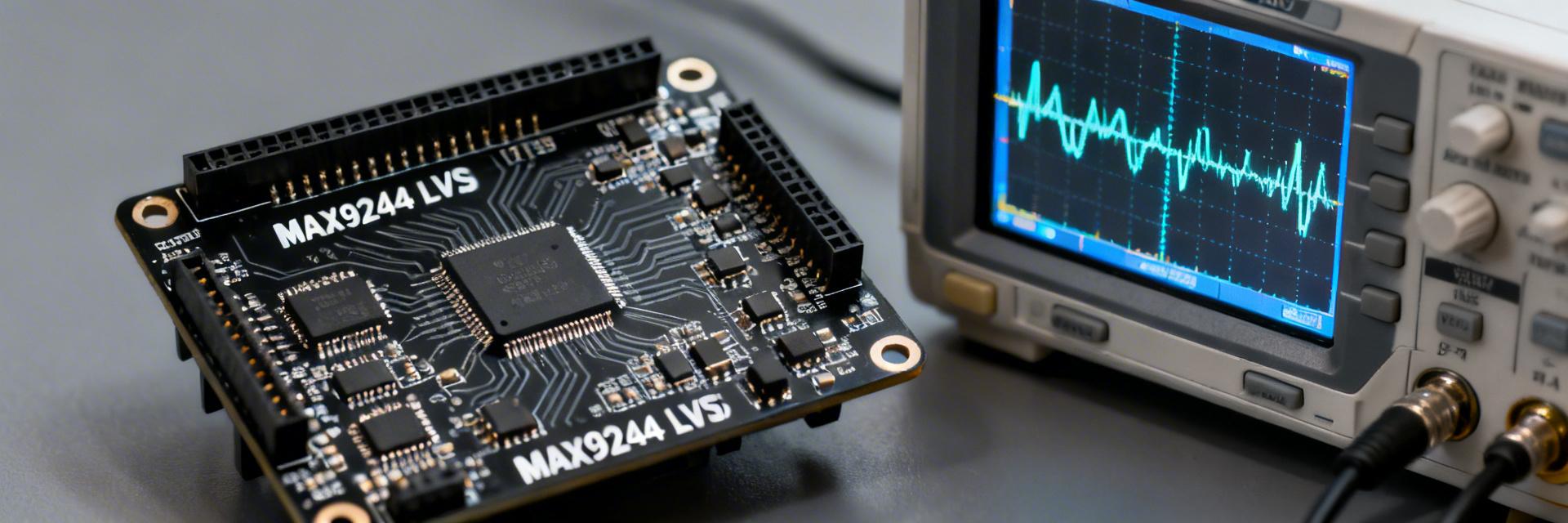
Point: A repeatable bench plan converts datasheet specs into pass/fail checks. Evidence: Recommended steps include controlled power sequencing, LVDS stimulus, proper termination, and environmental control as reflected by the device spec sections. Explanation: Execute power‑up with monitored rails, inject standard PRBS LVDS patterns at rated amplitude, capture differential waveforms with a 1 GHz scope and differential probe, check BER (target <1E‑12) and timing margins, and log results for each condition in a matrix (power, temp, stimulus amplitude).
4.2 Worst-case tests and margin verification
Point: Stress tests reveal fragile margins before field failure. Evidence: Datasheet absolute limits and ESD ratings guide stress bounds: sweep supplies across recommended window, exercise thermal chambers, and apply jitter injection to see crossover into failure modes. Explanation: Run supply tolerance sweeps and temperature steps while measuring BER and timing; if failure occurs near recommended limits, quantify margin and specify tighter design targets (e.g., tighten supply tolerance or add supervision) to ensure field reliability.
5 — Integration notes, layout tips & troubleshooting (case study / action)
5.1 PCB layout, decoupling, and grounding best practices
Point: Layout and bypassing dictate SI and thermal performance. Evidence: The datasheet recommends controlled impedance LVDS routing, termination placement, and decoupling near VCC pins. Explanation: Route LVDS as matched pairs with 100 Ω differential impedance, place termination at the receiver pin, cluster 0.1 μF and 1 μF bypass caps within 5 mm of power pins, and use thermal vias under the package where allowed to reduce Tj under sustained load.
5.2 Common failure modes and how to diagnose them
Point: Bit errors and thermal events have characteristic signatures. Evidence: Symptoms such as link flips, rising BER, or thermal shutdown map to termination faults, supply droop, or prior ESD events as implied by datasheet tolerances and ESD numbers. Explanation: Diagnose by checking differential eye amplitude, return loss, and supply ripple; a common case is missing termination causing collapsed eye—oscilloscope will show reduced differential amplitude and increased jitter, remedied by adding proper 100 Ω termination at the receiver.
Summary (Conclusion & Quick Action Checklist)
- Confirm headline limits: ~306 Mbps per link, 21 bits, 3.0–3.6 V supply, −40 to +85 °C, and ESD ±30 kV air.
- Respect electrical limits: Operate well inside absolute maxima; apply a 10–20% margin on supply and thermal budgets.
- Validate with structured tests: Use PRBS stimulus, differential probing, and BER targets (<1E-12) across temperature sweeps.
Frequently Asked Questions
What are the MAX9244 specs affecting system margins?
The core MAX9244 specs that drive margin are the per‑link data rate (~306 Mbps), recommended supply range (3.0–3.6 V), LVDS common‑mode window and termination requirement, and the operating temperature band. Test these in combination—supply tolerance, temperature, and injected jitter—to quantify usable margin before field deployment.
How should engineers verify electrical limits with bench tests?
Use a repeatable checklist: controlled power sequencing, PRBS LVDS stimulus at rated amplitude, 100 Ω termination at receiver, differential probing, BER measurement (target <1E‑12), and temperature sweeps. Log results in a pass/fail matrix and escalate failures to targeted remediation (termination, decoupling, or supervision).
Which layout steps most reduce bit errors for LVDS deserializers?
Prioritize matched differential routing with controlled impedance, place termination at the receiver, cluster bypass caps within a few millimeters of power pins, and keep noisy switching nets away from LVDS traces. These layout choices preserve eye height and timing, directly reducing BER and improving link robustness.