


MAX3232ESE+T: concise specs & sourcing report for engineers
MAX3232ESE+T: Concise Specs & Sourcing Report for Engineers
A Technical Evaluation and Procurement Guide for High-Performance RS-232 Transceivers
The MAX3232ESE+T is specified for single-supply operation from 3.0–5.5 V and implements a dual-driver/dual-receiver RS-232 transceiver with an internal charge pump using four external capacitors; the datasheet rates signaling up to ~250 kb/s. These facts matter when matching legacy UART links to low-voltage microcontrollers and planning PCB layout, power budgeting, and procurement for prototypes.
This report highlights the exact specs to confirm, common implementation pitfalls to avoid, and a pragmatic, risk-aware sourcing checklist for procurement and prototype runs. Engineers should cross-check the device datasheet for tolerances and verify any vendor claims with bench tests before production.
1 — Why MAX3232ESE+T matters (Background overview)
1.1 Core function and typical use-cases
Point: The device bridges TTL/CMOS UART levels and ±RS-232 signaling with two drivers and two receivers.
Evidence: It uses an internal charge pump to generate necessary RS-232 voltages from a single low-voltage rail.
Explanation: Typical applications include embedded serial ports, legacy instrument interfaces, industrial control panels, boot consoles, and test fixtures where microcontrollers need robust RS-232 links without an external ± supplies.
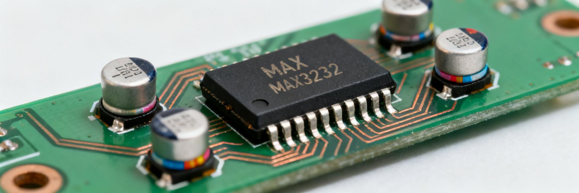
1.2 Key physical/package notes engineers must check
Point: Verify package variant and pin count before layout.
Evidence: The part is available in space-optimized surface-mount packages; the recommended land pattern in the datasheet controls thermal and solder reliability.
Explanation: Confirm exact package marking and ordering information, check the recommended footprint, and ensure thermal relief and paste-stencil settings match PCB assembly capabilities to avoid rework.
2 — Concise electrical specs & performance summary (Data deep-dive)
2.1 Power, signal levels and performance numbers to list
Point: Key electrical targets are supply range, current, output swing, and charge-pump caps.
Evidence: The primary supply range is 3.0–5.5 V; the device requires four external charge-pump capacitors (commonly 0.1 µF ceramics).
Explanation: Expect active supply current in the sub-mA to low-mA range and very low microamp-level shutdown current—verify typical and max values in the datasheet. The datasheet rates signaling up to ~250 kb/s; vendors sometimes list higher practical rates, so validate at intended baud.
| Parameter | Typical / Guidance |
|---|---|
| Supply | 3.0–5.5 V |
| Charge-pump caps | 4 × 0.1 µF ceramic (place close to device) |
| Rated data rate | ~250 kb/s (confirm for target baud) |
| Drivers / Receivers | 2 drivers, 2 receivers |
| Shutdown current | Microamp-class (datasheet: verify typical/Max) |
2.2 Timing, ESD and reliability items to call out
Point: Timing, ESD, and layout determine link robustness. Evidence: Propagation delays, driver/receiver enable behavior, and receiver thresholds are specified in the datasheet; ESD immunity ratings vary by model. Explanation: Note enable/disable line behavior for sleep modes, plan for ESD protection near connectors, follow decoupling rules, and treat cable length and capacitance as factors that reduce safe baud rate and signal margin.
3 — Implementation & typical circuits (Method / how-to)
3.1 Typical application schematic and BOM notes: A minimal BOM includes four charge-pump caps, a bypass cap, and the connector/cable interface. Recommended capacitor values and tolerances are in the datasheet; connector wiring follows standard TX/RX/RTS/CTS conventions. Use ceramic caps of specified value and voltage rating, place the charge-pump caps adjacent to the package, and document port idle states so firmware handles sleep/shutdown modes without leaving lines in ambiguous states.
3.2 PCB layout, grounding and EMI considerations: Layout impacts reliability and EMI. Evidence: Charge-pump caps and decoupling must sit close to pins; return paths and ground stitching reduce emissions. Route TX/RX traces as short controlled-impedance runs where possible, place ESD devices/chokes near the connector, and include test points for UART signals to speed field debugging and validation.
4 — Sourcing report for engineers (Procurement-focused)
4.1 Ordering codes, packaging and part marking: Confirm exact ordering code and packaging before purchase. Suffixes indicate tape-and-reel, temperature grade, lead finish, and packaging quantity. Verify moisture sensitivity level (MSL), RoHS/lead-free notation, and record exact part codes on POs.
4.2 Inventory signals and best practices: Watch inventory signals and enforce traceability. Mitigate risk by purchasing prototype and production quantities separately, require lot traceability on POs, qualify alternate sources, and specify shelf-life instructions to protect production schedules.
5 — Alternatives, counterfeit risks & compliance checklist
5.1 Pin-compatible alternatives: Evaluate alternatives by pinout, voltage, and timing. Shortlist by pinout first, then compare supply voltage range, data rate, power consumption, and thermal characteristics before qualifying substitutes.
5.2 Counterfeit/obsolescence mitigation: Implement incoming inspection. Require certificates of conformity, inspect package marking vs. datasheet, perform sample functional and ESD testing on incoming lots, and include RoHS/REACH declarations in supplier questionnaires.
Summary Checklist
- Confirm core specs: Single-supply 3.0–5.5 V, 2 drivers / 2 receivers, four external charge-pump capacitors.
- Design cautions: Place charge-pump and decoupling caps close to the device; account for cable capacitance at high baud rates.
- Procurement: Verify exact ordering codes, require lot traceability, and perform incoming functional tests.
FAQ
Is the MAX3232ESE+T suitable for low-voltage microcontroller UARTs?
Yes. The device is designed to translate between 3.0–5.5 V logic and RS-232 voltage levels. Engineers must confirm the exact logic thresholds and verify idle-line behavior during MCU sleep modes.
What charge pump capacitor values should be used with MAX3232ESE+T?
The typical recommendation is four external capacitors (0.1 µF ceramic) placed close to the device, plus a 0.1–1 µF bypass on VCC. Always verify the datasheet’s ESR guidance.
How should procurement guard against counterfeit MAX3232ESE+T parts?
Require supplier lot traceability and certificates of conformity, inspect package markings, and perform sample-test incoming lots functionally to reduce counterfeit risks.