


LT3093EMSE Pinout & Specs — Datasheet Summary for LDO
200mA Output
Ultra-Low Noise
The LT3093EMSE is a high-performance negative low‑dropout linear regulator optimized for precision analog systems.
Core Utility: This device supports an output range down to −19.5 V with a 200 mA maximum current capability. Its ultra‑low dropout of approximately 190 mV at rated load makes it indispensable for compact, programmable negative supplies such as sensor front-ends and op‑amp rails.
Quick Overview & Key Specifications
Application Context
Designed for precision negative rails, the LT3093EMSE features programmable control pins including PG/PGFB, VIOC, ILIM, and EN/UVLO. This combination is ideal for analog subsystems requiring adjustable current limits, power-good signaling, and controlled startup.
Package Details
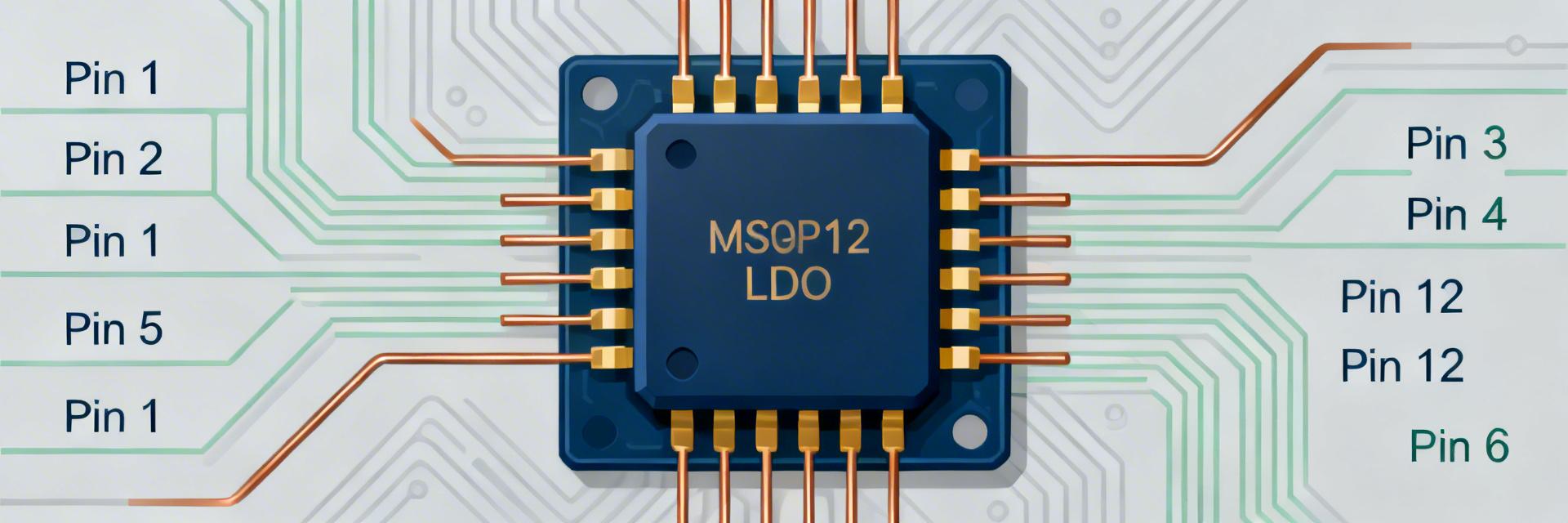
The device is housed in a 12-pin MSOP with an exposed thermal pad. Effective thermal management via PCB copper area and via stitching is critical for maintaining performance at the 200 mA rating.
Performance Visualization
100% Range
High Capacity
Ultra-Low Dropout
Pinout Analysis & Signal Functions
Input negative rail. Primary supply entry point.
Enable or Undervoltage Lockout.
Power-Good output and feedback monitoring.
Current-limit program pin via resistor.
Output clamp and offset control adjustment.
Program node and ground reference.
Output pins and Exposed Pad (Thermal Ground).
Electrical Characteristics Highlights
| Parameter | Typical / Max (Datasheet Specs) |
|---|---|
| Output Range | To −19.5 V (configured via SET resistor) |
| Maximum Output Current | 200 mA |
| Dropout Voltage (Typical) | ~190 mV at rated load |
| Quiescent Current | Refer to datasheet for specific VIN/VOUT conditions |
PCB Layout & Thermal Best Practices
- • Solder the exposed pad to a large copper plane with multiple thermal vias for heat dissipation.
- • Place input (1–10 μF) and output (4.7–22 μF) capacitors immediately adjacent to the pins.
- • Use star grounding for sensitive nodes (SET, VIOC) to prevent noise injection.
Common Troubleshooting
PG Stuck Low? Check PG pull‑up resistors and PGFB wiring.
Incorrect VOUT? Verify the SET resistor value and ensure VIOC connections are secure.
Thermal Shutdown? Increase copper area or derate current below 200 mA for sustained operation.
Common Questions (FAQ)
What is the LT3093EMSE pinout diagram for the 12‑pin MSOP?
+
How do you set VIOC on the LT3093EMSE?
+
What PCB layout tips ensure thermal reliability?
+