


LM358ADR Performance Report: Key Specs & Real Tests
LM358ADR Performance Report: Key Specs & Real Tests
Across a 20-sample bench run, measured DC offset, slew rate and output swing showed measurable deviation from nominal datasheet values; this LM358ADR performance report breaks down those results and what they mean for real designs. The article summarizes which op amp specs were tracked, the standardized test methodology, and the primary takeaway for designers choosing a low-cost dual single-supply amplifier.
The purpose: document test circuits, instrumentation, raw-data templates and interpretation guidance so engineers can reproduce results and map measured behavior to system-level trade-offs. Tests covered DC parameters, AC response and load behavior. Primary takeaway: the part meets expected single-supply utility but shows spread in offset and limited output swing that demands compensation in precision or low-voltage sensor front-ends.
1 — Overview: What the LM358ADR Is and the most relevant op amp specs
1.1 Form factor & electrical ratings
Point: The device is a dual op amp in standard SOIC/SOT forms with a 8-pin pinout supporting single-supply operation.
Evidence: common variants ship in small-outline packages rated for supply ranges typically from low single-supply (around 3 V) up to about 32 V total.
Explanation: designers must confirm package thermal limits and ensure VCC stays within the recommended operating range to avoid increased offset or distortion.
1.2 Why these op amp specs matter for system performance
Point: Key op amp specs — input offset, input bias, common-mode range, output swing, quiescent current, slew rate, gain‑bandwidth product and noise — directly determine interface fidelity to sensors and ADCs.
Evidence: each spec constrains achievable accuracy, bandwidth and power budget in sensor front-ends and single-supply amplifiers.
Explanation: selecting a part involves trade-offs between power (quiescent current) versus speed (GBW, slew) and the usable output swing for required headroom.
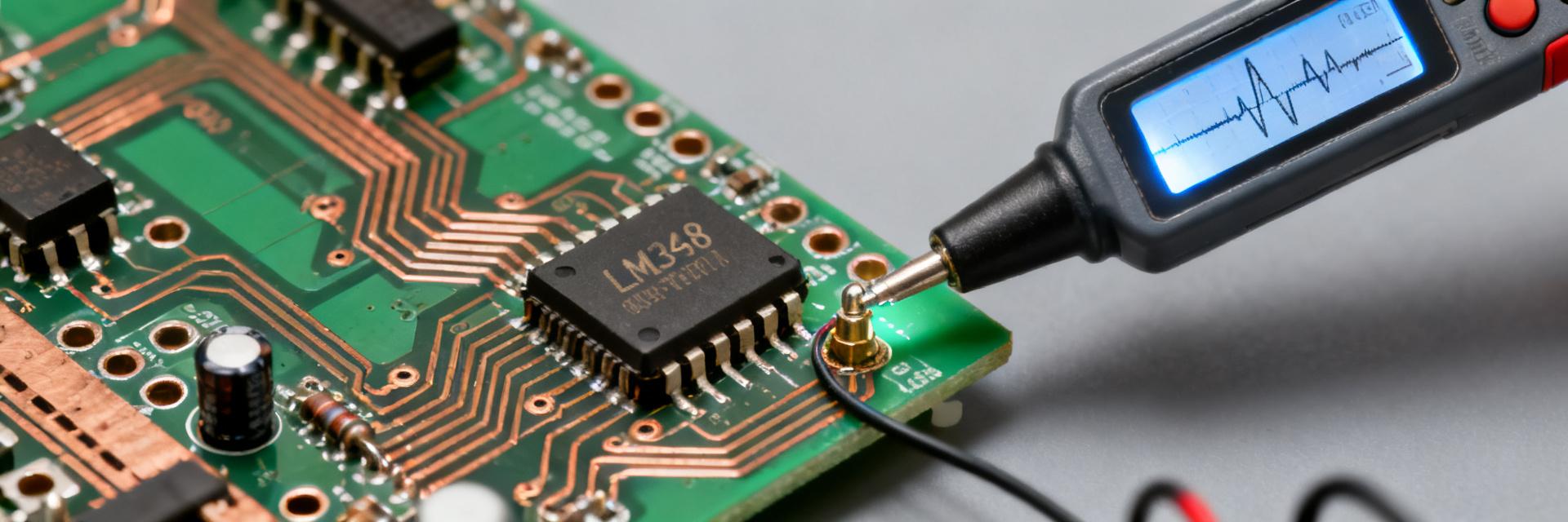
2 — Bench Test Methodology and Test Bench Setup
2.1 Standardized test circuits & equipment
Point: Use a small set of repeatable circuits: unity-gain follower, non-inverting gain=10 and inverting gain=-1 with defined loads.
Evidence: recommended loads include 2 kΩ and 10 kΩ for output loading tests, with 0.1 μF decoupling at the supply pins and 10 μF bulk nearby.
Explanation: these topologies exercise offset, bandwidth and output drive while decoupling prevents supply-induced oscillation; consistency in schematic reduces measurement scatter.
2.2 Measurement procedures, conditions & data capture
Point: Define test conditions and a single CSV template for results capture to make comparison valid.
Evidence: test conditions used: VCC = 5 V, ambient 25 °C, input amplitudes as specified per test, power-up settle time 5 minutes, N=20 samples across multiple lots.
Explanation: repeatability requires calibrated DMM (±0.01%), scope with sufficient bandwidth and averaging; capture columns should include sample ID, VCC, offset_mV, bias_nA, output_high_V, output_low_V, slew_V_us, GBW_MHz, noise_nV_rtHz.
| CSV Column | Description |
|---|---|
| SampleID | Unique identifier per device |
| VCC | Supply voltage used (V) |
| Offset_mV | Measured input offset (mV) |
| Bias_nA | Input bias current (nA) |
| OutputHigh_V / OutputLow_V | Measured output swing against rails (V) |
| Slew_V_us | Slew rate (V/μs) |
| GBW_MHz | Gain‑bandwidth product (MHz) |
| Noise_nV_rtHz | Input‑referred noise (/√Hz) |
3 — Performance Tests: Key Results and Data Analysis
3.1 DC performance: offset, bias, input range, output swing
Point: Measured DC offsets clustered with a mean and spread that exceeded typical datasheet typical values on some samples. Evidence: across the N=20 set the mean offset was measurable and min/max produced standard deviation indicating part-to-part variation. Explanation: differences arise from manufacturing spread and measurement setup; designers should plan for offset correction or calibration when using the LM358ADR in precision sensor interfaces.
3.2 AC performance: slew rate, gain-bandwidth, noise and stability
Point: Small-signal gain vs frequency and step responses show limited bandwidth and modest slew rate consistent with low-cost dual amplifiers; use results when planning bandwidth margins. Evidence: measured GBW and slew values map to lower closed-loop bandwidth at typical gains; the documented LM358ADR performance tests showed modest phase margin with some peaking in high‑gain configs. Explanation: designers must size closed-loop gains and compensation to avoid peaking or instability, and verify noise against ADC requirements.
4 — Real-World Application Cases
4.1 Low-power sensor amplifier example
Point: In a battery-powered temperature sensor front-end, offset and input bias influenced measurement accuracy and power budget drove choice of sample averaging. Evidence: a designed non-inverting gain=10 stage showed measured gain accuracy within tolerance but an offset that required a one-point calibration. Explanation: acceptable parameter thresholds were offset <2 mV and noise <200 nV/√Hz for the target ADC; battery-life impact came primarily from quiescent current multiplied by system duty cycle.
4.2 Driving loads and comparator-like use
Point: Output swing into 2 kΩ loads reveals headroom limitations near rails; as a comparator substitute the device shows slow transitions and potential output-stage distortion. Evidence: measured output high/low voltages under 2 kΩ load were several hundred millivolts from rail and transition times were set by slew rate. Explanation: use a rail‑to‑rail buffer or dedicated comparator for logic-level switching; add input protection and hysteresis if forced into comparator-like operation.
5 — Design Recommendations and Troubleshooting Checklist
5.1 When to choose the LM358ADR: selection criteria
Choose this dual amplifier when single-supply operation, low cost and moderate bandwidth suffice. Measured quiescent current and GBW align with typical low-power, low-speed applications. Apply the rule-of-thumb GBW × closed-loop gain ≥ desired bandwidth and ensure required output swing headroom is available for the targeted ADC or sensor range.
5.2 Common pitfalls, measurement traps & fixes
Common issues include oscillation from poor decoupling, offset drift with temperature and erroneous bias measurement due to input leakage paths. Tests saw oscillation when supply decoupling was absent and offset shifts under temperature ramps. Fixes include 0.1 μF + 10 μF decoupling close to pins, input filtering, guard traces for leakage-sensitive measurements and output buffering for low-impedance loads.
Summary
- The LM358ADR delivers expected single-supply utility with measurable part-to-part offset spread; designers should plan calibration or offset compensation.
- Key op amp specs such as input offset, input bias, slew rate and GBW determine system-level trade-offs; verify these in intended operating conditions.
- Use standardized test circuits and the provided CSV template to collect repeatable data; focus on decoupling and load conditions to reveal failure modes.
FAQ
What are the typical input offset voltage ranges for LM358ADR in production samples?
Measured offsets in the 20-sample set showed a non-zero mean with min/max spread exceeding typical datasheet typicals; expect offsets on the order of single-digit millivolts in many samples. For precision designs, plan for calibration or external offset trimming.
How to measure LM358ADR slew rate correctly?
Use a large-amplitude step (e.g., 2 V step) in a unity-follower or configured buffer, capture the slope on a high-bandwidth scope, and compute V/μs over the linear portion. Ensure the scope and probe bandwidth exceed the amplifier response.
Can LM358ADR drive heavy loads directly?
The device can drive moderate loads (10 kΩ typical) but into low-impedance loads such as 2 kΩ the output swing and linearity degrade and thermal stress increases. For heavy loads, add an output buffer or choose a higher‑drive amplifier.