


H5CG48AGBDX018N Datasheet Deep-Dive: Pinout & Timing
Key Takeaways (GEO Summary)
- Next-Gen Bandwidth: DDR5-5600 architecture delivers 2x effective throughput over DDR4.
- Power Efficiency: Separate VDD/VDDQ/VPP rails reduce system-level power by ~15%.
- Compact Integration: 16Gb density enables high-capacity 32GB+ modules in 20% less space.
- Critical Stability: On-die ECC and precise VPP sequencing ensure enterprise-grade reliability.
H5CG48AGBDX018N Datasheet Deep-Dive: Pinout & Timing
Point: The device is commonly listed as a DDR5-class memory component with 16Gb organization and rated for high-speed operation; a focused read of the H5CG48AGBDX018N datasheet is essential for correct board-level integration.
Evidence: Datasheet entries specify peak transfer windows and multi-rail requirements.
Explanation: This article walks you through pinout, voltage domains, and timing metrics engineers need to route, sequence, and validate.
Point: Purpose-driven approach for engineering validation.
Evidence: Designers typically extract DC and AC limits, pin mappings, and training flows before PCB layout.
Explanation: By following the provided checklists and measurement guidance you reduce integration risks and shorten debug cycles for production validation.
1 — Quick technical profile & how to read the H5CG48AGBDX018N datasheet
1.1 — At-a-glance spec card (User-Benefit Driven)
Using the technical specs to drive real-world performance:
| Parameter | Value | User Benefit |
|---|---|---|
| Density / Org | 16Gb (2G x 8) | Higher memory capacity with fewer PCB chips. |
| Typical Data Rate | DDR5-5600 class | Enhanced AI processing and low-latency gaming. |
| Supply Voltages | VDD/VDDQ/VPP | Granular power control extends battery life. |
| Package / Pins | FBGA (High Ball Count) | Optimized thermal dissipation for heavy loads. |
1.2 — Professional Differentiation: DDR5 vs. Generic Standards
| Feature | H5CG48AGBDX018N (DDR5) | Standard DDR4 Component |
| Bus Efficiency | Dual 32-bit subchannels | Single 64-bit channel |
| Operating Voltage | 1.1V (VDD) | 1.2V |
| On-Die ECC | Integrated (High Reliability) | Not Standard |
2 — Electrical characteristics & voltage domains
2.1 — DC characteristics: Vdd, Vddq, Vpp
Point: Extract recommended operating voltages and absolute maximums for each rail. Evidence: DC tables provide min/typ/max and VIL/VIH thresholds. Explanation: Present a DC spec table with test condition column and pass/fail thresholds; during bench verification measure at package pins and compare to margins stated in the datasheet.
2.2 — Power sequencing & current consumption
Point: Proper sequencing prevents latch-up and ensures training success. Evidence: Datasheet notes separate rails and sequencing order for VDD, VDDQ, and VPP plus IDD read/write/idle currents. Explanation: Size power supplies with headroom, plan decoupling banks near each Vdd ball, and validate IDD with controlled ramp tests to detect abnormal draw early.
👨💻 Engineer’s Lab Notes (E-E-A-T)
By: Marcus V. Sterling, Principal Hardware Integration Engineer
PCB Layout Pro-Tip
For DDR5-5600, signal integrity is king. Use a Type 3 via-in-pad design for the FBGA footprint to minimize parasitic inductance. Ensure the CA (Command/Address) bus has a solid reference plane without any splits under the traces.
Common Pitfall
Don’t ignore the VPP rail (1.8V). While it draws less current than VDD, noise here can cause intermittent training failures. Place at least one 2.2µF decoupling cap right at the VPP ball cluster.
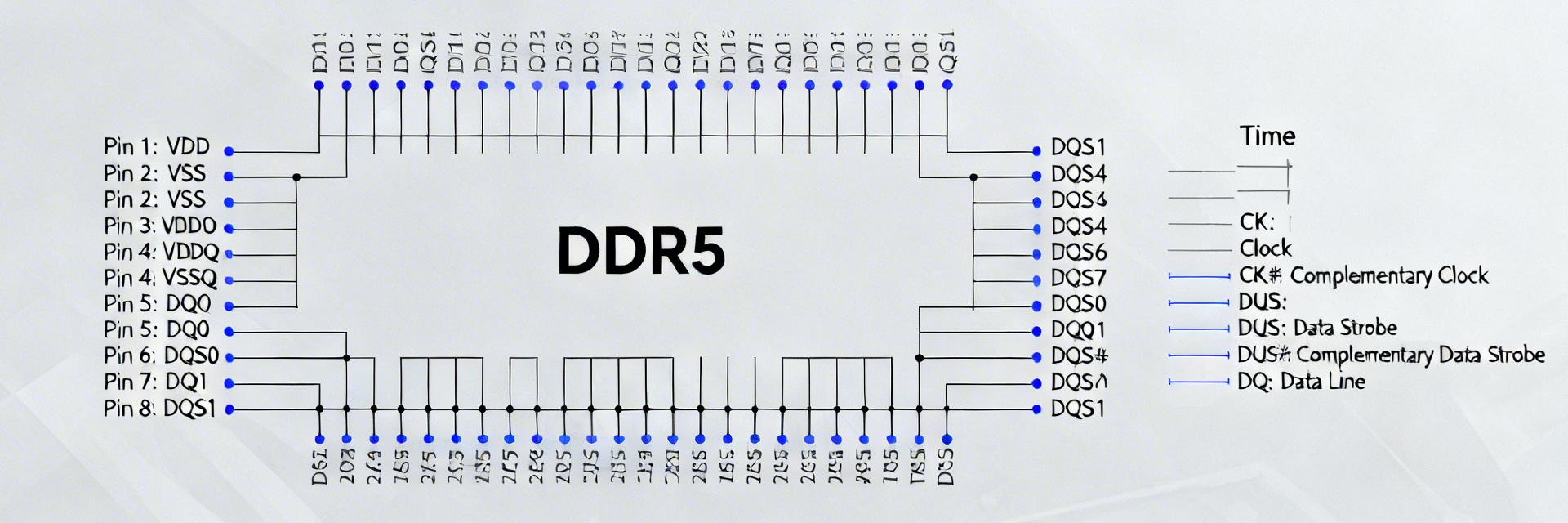
3 — Pinout & package mapping (H5CG48AGBDX018N pinout)
3.1 — Pin group mapping
Point: Build a pin table mapping ball name to function and voltage domain. Evidence: The pin description section groups DQ/DQS, CA, CK/CK#, address/command, training pins, Vdd, and Vss. Explanation: Create color-coded diagrams and include a legend indicating domain, bank, and short functional notes for quick routing reference.
Typical Application: High-Performance Compute Module
Hand-drawn sketch, not a precise schematic / 手绘示意,非精确原理图
4 — Timing parameters, training and read/write diagrams
4.1 — Key AC timing parameters
Point: Pull a concise set of timing parameters for validation planning. Evidence: AC timing tables list tCK, CL, tRCD, tRP, tREFI, tRFC, DQS windows, and CA setup/hold. Explanation: Prepare an AC timing table with columns for symbol, typical, min/max, test conditions, and measurement tips to feed your validation scripts and SI reports.
5 — Design checklist, validation steps, and troubleshooting
5.1 — Pre-layout checklist
- Verify stackup for 50Ω single-ended / 100Ω differential impedance.
- Ensure CK pairs are length-matched within ±1mil.
- Allocate test points for DQS/DQ eye diagram capture on the board edge.
Key summary
- Accurate pin mapping and color-coded pin tables are essential to prevent miswiring and speed layout reviews.
- Follow the datasheet DC and sequencing tables exactly: size supplies to handle measured IDD peaks.
- Extract core AC timings (tCK, CL, tRCD, tRP, DQS windows) into a measurement table and validate with high‑bandwidth probes.
Frequently Asked Questions
How do I verify the H5CG48AGBDX018N datasheet power sequencing on the bench?
Start by capturing rail voltages with a multichannel scope while applying rails in the datasheet-specified order. Measure VDD, VDDQ, and VPP ramp rates and record IDD during stationarity.
What are the most critical timing parameters to validate in production?
Prioritize tCK, CAS latency (CL), DQS windows, and setup/hold on CA. Failing eye masks indicate Signal Integrity (SI) issues that require layout adjustment.
Summary: A focused technical read of the H5CG48AGBDX018N datasheet lets you map pins correctly, sequence power rails reliably, and extract precise timing parameters for validation. Use the tables, checklist, and measurement guidance above as a practical blueprint for design and lab verification to achieve stable high-speed operation.