


BL1117-33CY Datasheet Deep Dive: Pinout, Specs & Notes
BL1117-33CY Datasheet Deep Dive: Pinout, Specs & Notes
A comprehensive technical guide for engineers on integrating the 3.3V low-dropout linear regulator.
The regulator under review is a fixed 3.3 V low-dropout linear regulator commonly used where simplicity and low noise matter. Typical published figures to set context: nominal output 3.3 V, maximum output current around 0.8–1.0 A, dropout that grows with load (≈0.3 V at light load, approaching ~1.0–1.2 V near maximum current), quiescent current in the single-digit milliamps, and PSRR that improves at mid-to-low frequencies. These metrics drive decisions in power budgeting, thermal design, decoupling and noise-sensitive analog front ends, so designers should confirm exact numbers from the official datasheet for the package and revision in use.
This article is a practical, data-driven walkthrough of the regulator’s datasheet, pinout, design rules and test notes so engineers can integrate the device reliably. It highlights the electrical limits and corner cases, pinout and footprint recommendations, decoupling and thermal calculations, a concise test plan, and a worked example that ties the numbers together. The term “datasheet” is used throughout to signal where to verify exact test conditions and limits.
1 — BL1117-33CY at a glance (Background introduction)
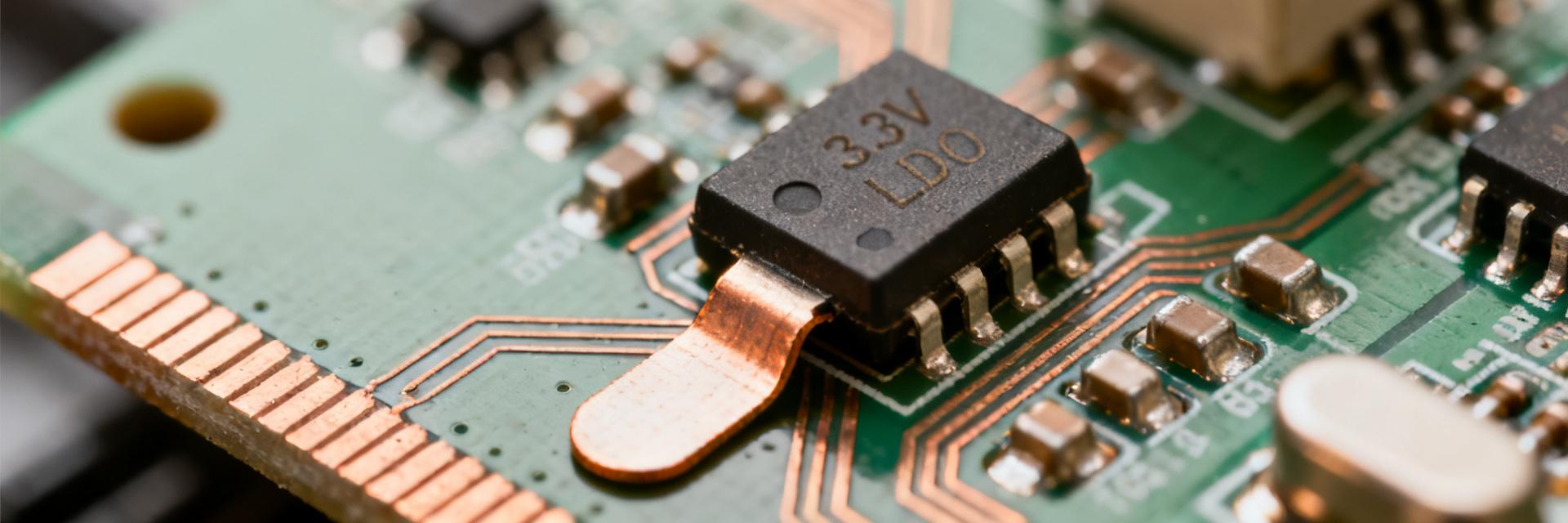
Key specs summary
| Parameter | Typical / Max | Test condition / note |
|---|---|---|
| Nominal VOUT | 3.3 V | Tj = 25°C, fixed device |
| Max output current | ≈ 0.8–1.0 A | Package and PCB thermal limits apply |
| Input voltage range | VIN ≥ VOUT + dropout; up to ~15 V abs. max | Observe absolute max VIN in datasheet |
| Dropout voltage | ~0.3 V @ 100 mA; ~0.9–1.2 V @ 800–1000 mA | Measured at 25°C |
| Quiescent current (Iq) | single-digit mA | Depends on load and temperature |
| PSRR (120 Hz) | ~50–70 dB | Varies with load and frequency |
| Output noise | low μV–mV range | Depends on caps and bandwidth |
| Max junction / operating temp | ~125°C junction; operating range per datasheet | Follow derating guidance |
| Common packages | SOT-223, DPAK (TO-252), through-hole variants | Package affects thermal resistance |
Typical use cases & where it fits in designs
Applications include powering microcontrollers, sensor clusters, low-speed radios and small communication modules where low noise and minimal BOM are priorities. The linear regulator trades efficiency for simplicity: compared with switching converters it requires fewer components and produces less high-frequency switching noise, but dissipates more power as heat when VIN − VOUT and IOUT are large. Choose it when noise, board space, or transient response outweigh absolute efficiency.
2 — Datasheet deep-dive: electrical characteristics & limits (Data analysis)
Absolute maximum ratings & recommended operating conditions
Absolute maximums typically include a maximum VIN (often ≤ 15 V), maximum junction temperature (≈125°C), and maximum power dissipation determined by package thermal resistance. Recommended operating conditions constrain VIN above VOUT by the dropout margin plus margin for tolerance. Respect absolute ratings to avoid catastrophic failure and long-term reliability loss; apply derating (e.g., 50–75% of max power dissipation) and plan for temperature margin in ambient and enclosure conditions.
Electrical characteristics explained
Key electrical rows to inspect: output tolerance (initial and over temperature), line and load regulation, minimum load (if required for regulation), dropout vs current curve, short-circuit/current limit behavior, thermal shutdown threshold and hysteresis, quiescent current and PSRR/noise figures. Use these numbers in calculations: select VIN ≥ VOUT + maximum dropout + tolerance stack-up; calculate worst-case VOUT = nominal ± tolerance at min/max Tj; and include current-limit and thermal shutdown when planning transient behavior.
3 — Pinout, package options and footprint recommendations (Data + practical)
Pin functions and typical pin mapping
Typical fixed 3.3 V devices use a three‑lead pinout: IN, GND (or ADJ in adjustable versions), and OUT. In common packages the metal tab is tied to ground; confirm the package drawing in the datasheet. Protect the input pin from large reverse or transient voltages—add an input diode or series protection if the source can be connected incorrectly or if hot-plugging is expected. Keep sensitive loads referenced to the same ground plane to avoid ground bounce.
Package variants and PCB footprint notes
Popular packages include small SMD packages (e.g., SOT‑223), DPAK/TO‑252 and through‑hole types. Thermal vias beneath the thermal pad or tab are critical: use an array of vias (e.g., 4–12) tied to a large copper pour to spread heat. Keep IN and OUT traces short and place the input bulk capacitor close to VIN pin and ground. Follow the datasheet land pattern recommendations and use consistent solder paste to avoid tombstoning or poor thermal contact.
4 — Design & application guidelines (Method / How-to)
Decoupling and Capacitors
Datasheet stability requirements usually mandate an output capacitor with a minimum capacitance and a suitable ESR range. A practical baseline: 10 μF low‑ESR electrolytic or tantalum on the output plus a 0.1 μF ceramic at the pins for high-frequency decoupling. If ESR is too low or too high the regulator can oscillate—adhere to the recommended range.
Thermal Management
Estimate power dissipation Pd = (VIN − VOUT) × IOUT. Use package θJA or θJC from the datasheet to compute junction rise: ΔTj = Pd × θJA. For example, with VIN = 5 V, VOUT = 3.3 V and IOUT = 0.8 A, Pd = 1.36 W; with θJA ~ 50°C/W, ΔTj ≈ 68°C above ambient — likely requiring board copper for heat spreading.
5 — Testing, common issues & a quick example application (Case + action)
Test procedures & measurement tips
A concise test plan: verify no-load VOUT, then load to target current and full rated current while monitoring VOUT, VIN and case temperature; perform dropout test by reducing VIN until regulation fails; run a thermal soak at expected ambient and load; measure output noise/PSRR using the datasheet bandwidth and same decoupling. Use a short ground spring or Kelvin probe for scope ground to avoid injecting noise.
Common failure modes & troubleshooting
Frequent issues include instability from inappropriate output cap ESR, overheating when VIN − VOUT is large at high IOUT, incorrect pin connections, and inadequate thermal vias. Troubleshoot by checking cap types, swapping to higher-capacity copper pours, and verifying pin mapping with continuity tests. Example: to power a 3.3 V microcontroller cluster drawing 0.6–0.8 A from a 5 V rail, select VIN = 5 V, output caps 10 μF low‑ESR + 0.1 μF ceramics, expect Pd ≈ 1.02–1.36 W and validate thermal margin.
Conclusion
Key takeaways: the regulator provides a simple, low‑noise 3.3 V supply with up to ~0.8–1.0 A capability but requires attention to dropout, thermal dissipation and output‑cap ESR for stable operation. Verify absolute maximums and thermal resistances in the official datasheet for your chosen package, follow recommended footprint and decoupling, and perform the suggested tests (dropout, thermal run‑in, PSRR). Designers must validate parts in their exact package and operating environment to ensure reliable integration of the BL1117-33CY.
Key summary
- Check the datasheet’s dropout vs current curve and plan VIN so VOUT remains within tolerance across temp and load; account for tolerance stack‑up and headroom when selecting VIN.
- Follow capacitor recommendations: a low‑ESR 10 μF output cap plus a 0.1 μF ceramic at the pins is a practical starting point to ensure stability and low noise under varying loads.
- Estimate Pd = (VIN − VOUT)×IOUT and use θJA/θJC to size board copper or a heatsink; thermal vias and a solid ground pour greatly improve dissipation for SMD packages.
FAQ
What thermal calculation should I run before placing the regulator?
Compute Pd = (VIN − VOUT) × IOUT for worst‑case current, then ΔTj = Pd × θJA (from the datasheet) to estimate junction temperature rise above ambient. Add ambient and margin; if Tj approaches the datasheet limit, increase copper, add vias or use a larger package/heatsink. Validate with a thermal soak test under realistic enclosure conditions.
How do I verify dropout behavior referenced in the datasheet?
Set up a test where VIN is slowly reduced while the device supplies the target load current; record VIN at which VOUT falls by a specified regulation band (per datasheet definition). Use the same temperature and decoupling conditions as the datasheet test to obtain comparable numbers, and repeat at several load currents to map dropout vs current.
Which decoupling capacitors meet the datasheet stability requirements?
Follow the datasheet’s minimum capacitance and ESR range—typical practical choice is a 10 μF low‑ESR electrolytic or tantalum on the output combined with a 0.1 μF ceramic at the pins. If long VIN traces or high ripple sources are present, increase input bulk capacitance and place ceramics close to the pins to reduce impedance at high frequency.