


93LC56B EEPROM: Complete Pinout & Electrical Specs
93LC56B EEPROM: Complete Pinout & Electrical Specs
Point: The 93LC56B EEPROM is a low-voltage, serial nonvolatile memory often used for small configuration and calibration storage.
Evidence: Typical datasheet shows ~2 Kbit organized as 128×16 words, VCC ranges near 2.5–5.5 V, and write endurance on the order of 1,000,000 cycles.
Explanation: These characteristics make the part attractive for battery-backed and low-power embedded systems; verify the exact marking for revision differences. 93LC56B-ISN
Point: This reference distills pinout, electrical specs, command timing, integration tips and a test checklist into a concise technical reference.
Evidence: Numbers referenced are representative device values drawn from official datasheet tables; use the exact datasheet for production.
Explanation: Use the pin mapping and timing sequences here as implementation anchors for firmware and PCB design.
1 — Background: what the 93LC56B EEPROM is and where it fits
Memory organization & device variants
Point: The device labeled as the 56B variant is a 2-Kbit serial EEPROM commonly organized as 128 words of 16 bits (x16); x8 variants exist with identical addressing but half-word width.
Evidence: Datasheet addressing width and ORG selection bits determine whether the bus presents x8 or x16 words.
Explanation: Firmware must adapt address width and data packing; an ORG/width-select pin (when present) switches internal word organization, affecting read/write word boundaries and address bit counts.
Typical electrical & performance summary (quick specs)
Point: Key operating ranges include VCC ≈2.5–5.5 V, maximum clock in the low MHz range, typical standby/read/write currents in microamp-to-milliamp range, and data retention on the order of decades.
Evidence: Representative timing and ICC rows in datasheets define conditions (VCC, TA) for listed numbers.
Explanation: For reliability, dimension decoupling, watch current during write cycles, and select industrial temperature grade when extended range is required.
2 — Pinout & package options for the 93LC56B EEPROM
How to present a clear pinout (recommended table & diagram)
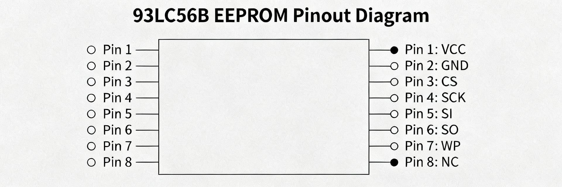
Point: A clear implementation uses an 8-pin diagram plus a table mapping pin number → name → function: CS (chip select), SK (serial clock), DI (data in), DO (data out), ORG (word-size select if present), VCC, GND, and NC/pull state. Evidence: Most 8‑pin serial EEPROMs follow this convention and datasheets list identical nets. Explanation: Place a PCB silk diagram and the table near the schematic to avoid miswiring; treat NC pins as no-connect unless the datasheet says otherwise.
| Pin # | Name | Function |
|---|---|---|
| 1 | CS | Chip select / active low input that frames serial transfers |
| 2 | SK | Serial clock input (microwire-style) |
| 3 | DI | Data in (MSB first during commands) |
| 4 | GND | Ground reference |
| 5 | DO | Data out (tri-stated when CS high) |
| 6 | ORG | Organization select (when implemented) |
| 7 | VCC | Supply voltage |
| 8 | NC | No connect or manufacturer-defined |
Common pin-level gotchas and application notes
Point: Idle and active levels matter: CS is typically active low, clocks are sampled on defined edges, and DO is tri-stated when CS is inactive. Evidence: Datasheet timing diagrams show tCS and bus-release timing. Explanation: Use a defined pull-up or pull-down on CS to prevent accidental writes; if an ORG pin exists, tie it deliberately to the required logic level and document for production.
3 — Electrical specs: absolute ratings, recommended operating conditions, DC/AC characteristics
Absolute maximum ratings & recommended operating conditions
Point: Absolute limits must be treated as destruction thresholds: VCC max, input voltages relative to VCC and ground, and storage temperature. Evidence: Datasheets list absolute maximum tables separate from recommended operating ranges. Explanation: Define operating margins (e.g., avoid running at absolute VCC max), include proper decoupling, and plan derating for extended reliability or automotive/industrial grades.
DC and AC characteristics to document
Point: Document ICC in standby/read/write modes and the AC timing: fCLK max, tCS, tCLK high/low, setup/hold, tWR (write cycle time) and program pulse widths. Evidence: Typical device tables give these values at specified VCC and TA. Explanation: Specify test conditions with each numeric spec in design docs and use conservative timing in firmware to ensure reliable write/erase completion.
4 — Interface, commands and timing sequences
Command set overview and framing
Point: The serial Microwire-style interface uses CS framing and clocked command bits; operations include read, write (word program), and EWEN/EWDS (write enable/disable). Evidence: Opcode patterns and address widths are defined in datasheets for the device organization. Explanation: Implement MSB-first transmission, respect address bit length based on ORG, and require EWEN before program sequences to avoid accidental writes.
Example transfer sequences & timing diagrams
Point: A typical read: pull CS low, shift opcode+address MSB-first, then clock out data bits; a write: EWEN, CS low, opcode+address+data, then wait tWR and verify. Evidence: Timing diagrams in the datasheet show required CS setup/hold and clock timing. Explanation: In firmware, implement a read-verify after write and use conservative delays or polling of a status bit where supported.
5 — Practical use cases & example implementations
Typical application scenarios
Point: Common uses are storing device configuration, small lookup tables, MAC/ID or calibration constants, and boot flags. Evidence: The device’s endurance, retention and low-voltage operation suit occasional writes and long-term read access. Explanation: Use it where small nonvolatile storage suffices; for frequent runtime logging or large datasets, choose higher-capacity or wear-leveling solutions.
Example integration snippets (hardware + firmware notes)
Point: Hardware connections are straightforward: CS to a GPIO, SK to a clock pin, DI/DO to MOSI/MISO or GPIOs, VCC and GND routed with decoupling. Evidence: Reference schematics in datasheets show these connections. Explanation: Firmware pseudocode: assert CS low → shift opcode+address → for i in bits: toggle SK, sample DO → deassert CS; for writes include EWEN and tWR wait plus read-verify.
6 — Troubleshooting, testing & PCB-integration checklist
Common failure modes and diagnostic steps
Point: Symptoms include no response, all-FF or all-00 reads, or intermittent corruption. Evidence: These behaviors map to wiring, power, or timing faults noted in field reports and datasheet cautions. Explanation: Troubleshoot by measuring VCC at the device, probing CS/SK/DI/DO waveforms with the scope, confirming pull resistor values and logic levels, and verifying ORG pin state.
PCB layout and test checklist before first power-up
Point: Prior to power-up, verify decoupling within 5 mm of VCC pin, short ground returns, clear routing for clock/data, and ESD protection on exposed headers. Evidence: Standard layout best practices reduce noise-induced failures. Explanation: Include a production test: write–read verify routine, voltage boundary checks, and an endurance sample to catch early-life failures.
Summary
Point: The 93LC56B EEPROM is a compact, low-voltage serial memory well suited for configuration and calibration storage. Evidence: Representative datasheet figures support the 2-Kbit x16 organization, low-voltage range and finite write endurance. Explanation: Use the pinout and timing guidance here as implementation anchors and validate all numeric values against the exact device datasheet before production. 93LC56B-ISN
Key summary
-
✔
The 93LC56B EEPROM provides ~2 Kbit (128×16) nonvolatile storage; confirm ORG pin state and address width in firmware and hardware documentation for correct read/write granularity. -
✔
Critical electrical specs: operate within recommended VCC (≈2.5–5.5 V), respect clock frequency limits in the datasheet, and budget for program time (tWR) and write currents during design. -
✔
Integration checklist: tie CS to a defined idle level, add local decoupling, route clock/data cleanly, implement EWEN flow for writes, and always perform read-verify after programming.
FAQ
What is the addressable word size of the 93LC56B EEPROM?
Answer: The 93LC56B EEPROM typically presents 128 words of 16 bits (x16) in the “B” organization; some variants expose x8 organization selectable by ORG. Check the device marking and datasheet to determine whether addresses are word or byte indexed and adjust firmware address math accordingly.
How do I select x8 vs x16 organization for the 93LC56B EEPROM?
Answer: Organization is selected either by a dedicated ORG pin or by the specific device ordering code; the ORG pin logic level or the device variant determines whether the interface expects x8 or x16 words. Confirm the intended organization in the datasheet and tie the ORG pin to a defined logic level on the PCB.
How to verify a successful write operation to the 93LC56B EEPROM?
Answer: After the write sequence and tWR interval, perform a read-back of the written address and compare words; for added robustness implement a CRC or checksum for multi-word writes. If available, use any device-ready polling or status response; otherwise use conservative delays and verify data integrity across voltage ranges.