


P24C04C-SSH-MIR Datasheet: Pinout & PCB Footprint Guide
P24C04C-SSH-MIR Datasheet: Pinout & PCB Footprint Guide
Point: The P24C04C-SSH-MIR is a 4-Kbit (512 x 8) I2C EEPROM that operates from approximately 1.7 V to 5.5 V and supports high-speed I2C modes, making it a compact nonvolatile option for configuration and calibration storage.
Evidence: The device family specifies 4-Kbit organization, single-supply operation approaching 1.7 V, and high-speed clocking up to 400 kHz or 1 MHz depending on variant in the EEPROM datasheet.
Explanation: These electrical and timing characteristics directly affect pin-level decoupling, pull-up resistor selection, and trace-length constraints when creating a reliable PCB footprint for system integration.
Point: This guide delivers a clear pinout breakdown, an IPC-aligned land-pattern creation method, layout best practices, and a production validation checklist to minimize rework.
Evidence: Practical steps reference standard mechanical drawing elements and IPC footprint classes while aligning with common production failure modes.
Explanation: Designers following these steps can drop the part into boards with reduced risk of tombstoning, bridging, and signal-integrity issues, accelerating time-to-first-test.
Quick device overview & key specs (background)
Device summary & electrical highlights
Point: Core specs determine board-level choices.
Evidence: The memory organization is 512 x 8 (4 Kbit); rated VCC range spans low-voltage single-supply operation near 1.7 V up to 5.5 V; supported I2C clock rates include standard/fast and high-speed variants, with endurance and data retention values defined in the EEPROM datasheet.
Explanation: Low-voltage capability means decoupling placement and pull-up resistor values must accommodate borderline thresholds, while supported clock rates govern allowable trace length and pull-up strength for reliable ACK timing.
Package types & mechanical overview
Point: Typical package forms for this family are 8-pin gull-wing surface-mount types that require precise land patterns.
Evidence: Mechanical drawings list overall outline, pin pitch (commonly 1.27 mm for smaller 8-pin variants or 1.27/1.27 mm family pitches), lead width, and recommended land pattern references.
Explanation: Designers must extract pin pitch and lead dimensions from the mechanical drawing to create an IPC-aligned footprint and verify courtyard and keepout clearances before releasing Gerbers.
Pinout explained: functions & electrical notes (data-analysis)
Pin functions & signal descriptions
Point: A correct pin map prevents orientation and wiring faults.
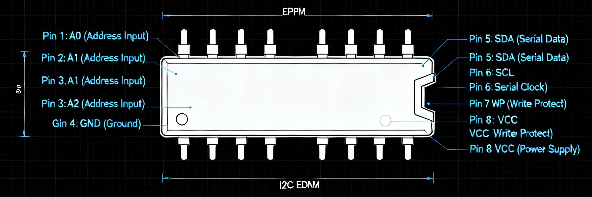
Evidence: Typical pin list includes VCC (power), GND, SCL (I2C clock), SDA (I2C data), address inputs (A0/A1/A2) if present, and WP (write-protect).
Explanation: VCC requires close decoupling to GND; SDA/SCL need pull-ups to VCC sized per bus capacitance and speed; A‑pins can be tied to VCC/GND or left floating only per datasheet guidance; WP behavior (active high or low) must be wired to meet intended write-protect policy.
Timing & I2C electrical considerations
Point: Timing parameters set layout constraints.
Evidence: Supported clock rates (400 kHz / 1 MHz variants), write cycle times, and ACK timing are specified in timing tables within the EEPROM datasheet.
Explanation: Higher clock rates require lower pull-up values and shorter traces; write-cycle delays imply software-level wait or polling; on multi-node buses, place optional series resistors and consider ESD diodes or common-mode filtering for robustness.
| Pin # | Name | Type | Function |
|---|---|---|---|
| 1 | A0 | I | Address input / board configuration |
| 2 | A1 | I | Address input / board configuration |
| 3 | A2 | I | Address input / board configuration |
| 4 | GND | P | Ground |
| 5 | SDA | I/O | I2C data; open-drain, requires pull-up |
| 6 | SCL | I | I2C clock; open-drain, requires pull-up |
| 7 | WP | I | Write-protect; follow datasheet polarity |
| 8 | VCC | P | Supply voltage |
PCB footprint & land-pattern creation (method guide)
Creating an IPC-aligned footprint
Point: Extracting precise dimensions yields manufacturable footprints.
Evidence: Datasheet mechanical drawings provide pin pitch, pad size, toe/heel details, and recommended land patterns; IPC footprint classes (Least/Moderate/Most) guide tolerances.
Explanation: Select an IPC class based on assembler capabilities; compute pad length/width from lead dimensions, add pad-to-pad clearance per solder joint geometry, and include a clear courtyard and placement outline. Export a STEP for MCAD/ECAD checks.
Solder mask & paste stencil
Point: Paste aperture design impacts solderability.
Evidence: Standard guidance suggests 60–80% pad solder paste coverage for small gull-wing leads and considers rectangular or trapezoid apertures to minimize bridging.
Explanation: Use truncated rectangles or multiple apertures to prevent excess solder; consider non-solder mask defined vs solder mask defined pads per PCB stack-up; confirm final values against the mechanical drawing before CAM.
| Feature | Sample value (mm) |
|---|---|
| Pin pitch | 1.27 |
| Pad length | 1.6 |
| Pad width | 0.5 |
| Paste coverage | 65% |
PCB layout best practices & DRC checks (method/guide)
Placement & routing recommendations
Point: Good placement minimizes signal problems.
Evidence: Best practices place EEPROMs close to the I2C master, route SDA and SCL as short, parallel traces, and keep them away from switching power or high-speed clocks.
Explanation: Position decoupling (0.1 μF) adjacent to VCC and GND pins; place series resistors close to the chosen end of the bus; avoid vias in immediate pad landings when possible to reduce assembly risk.
DRC and pre-production checks
Point: Automated checks catch common footprint mistakes.
Evidence: Run DRC for trace-to-pad clearance, paste mask conflicts, silkscreen overlaps, and courtyard violations; perform 3D collision and Gerber verification.
Explanation: Use IPC footprint verification tooling or a checklist to ensure paste apertures do not overlap and that pin 1 orientation is clear, preventing orientation mismatches on the SMT line.
Validation checklist, common issues & production tips (case/action)
Common problems and quick fixes
Point: Typical failures are avoidable with focused fixes.
Evidence: Observed issues include pin-1 misorientation, improper pad sizing causing tombstoning, missing decoupling, and incorrect address wiring.
Explanation: Mitigations include verifying pin-1 silkscreen and courtyard, adjusting pad geometry or paste coverage, adding solder thieving, confirming decoupling placement, and validating A-pin wiring against intended address map.
Pre-production validation checklist
Point: A final sign-off prevents costly re-spins.
Evidence: Checklist items should include verifying footprint vs mechanical drawing, running paste mask CAM checks, confirming reflow profile with assembler, and validating pull-up resistor values for the intended I2C speed.
Explanation: Assemble a small prototype run, perform power-up checks, and execute basic read/write I2C tests and continuity checks prior to full production.
Summary
Point: Correct pinout interpretation and an IPC-aware PCB footprint reduce assembly issues and speed testing.
Evidence: Applying the datasheet’s mechanical details, following IPC pad guidance, and validating paste/aperture choices mitigates common failures for a 4-Kbit I2C device like the P24C04C-SSH-MIR.
Explanation: Always cross-check the official EEPROM datasheet mechanical drawing before generating production Gerbers and choose pad and stencil parameters to match assembly capability for reliable first-pass yields.
- Extract mechanical dimensions and pin pitch from the EEPROM datasheet before footprint creation to ensure correct P24C04C-SSH-MIR pad geometry.
- Use IPC footprint classes to set tolerances and choose paste coverage (60–80%) to reduce bridging and tombstoning risks.
- Place the device close to the I2C master, keep SDA/SCL short, and locate a 0.1 µF decoupling capacitor adjacent to VCC/GND pins.
Common questions
How should I wire A0/A1/A2 for the P24C04C-SSH-MIR on my PCB?
Point: Address pins define the device address.
Evidence: The datasheet shows A‑pins can be tied to VCC or GND to set the lower bits of the slave address or left per variant guidance.
Explanation: Route A-pins to solder jumpers or pads for flexibility in prototypes; for production, hardwire to the intended logic level and document the resulting I2C address to avoid bus conflicts.
What is the recommended decoupling and power layout for P24C04C-SSH-MIR?
Point: Decoupling ensures stable VCC under write and bus activity.
Evidence: Low-voltage operation increases sensitivity to supply transients; datasheet recommends local decoupling.
Explanation: Place a 0.1 µF ceramic capacitor as close as possible between VCC and GND pins with short vias to the ground plane and use ground stitching to reduce impedance for optimal write reliability.
Which PCB footprint class should I choose for the P24C04C-SSH-MIR?
Point: Footprint class balances yield and assembly capability.
Evidence: IPC classes (Least/Moderate/Most) correspond to tighter or looser tolerances and assembler capability.
Explanation: For most contract assemblers choose IPC-Moderate; if using high-precision in-house assembly select IPC-Most; always validate the generated footprint against the device mechanical drawing and assembler capabilities before ordering PCBs.