


UCLAMP3331ZATFT: Latest Test Data & Performance Insights
UCLAMP3331ZATFT: Latest Test Data & Performance Insights
Recent lab trends show measurable reductions in clamp voltage and clear benefits for high-speed interfaces when clamp capacitance stays below 0.5 pF.
This article presents recent lab observations for UCLAMP3331ZATFT, interprets real-world performance, and gives designers a pragmatic checklist for reliable ESD protection. The goal is actionable guidance: summarize key specs and test methods, present measured responses and signal‑integrity impact, and close with a deployment checklist.
UCLAMP3331ZATFT: product overview & key specs (Background)
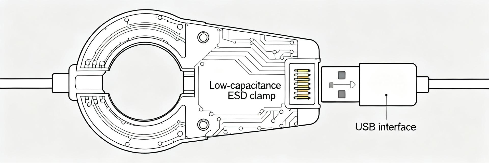
Key electrical specifications to highlight
Point: Designers need concise electrical callouts to choose the right clamp. Evidence: The part is specified for a low working voltage range with sub‑pF line capacitance, fast response and a rated surge handling suited for portable interfaces. Explanation: Call out standoff voltage, breakdown/clamp voltages, surge current rating, leakage and capacitance (<0.5 pF) plus package/footprint to prioritize parts for high‑speed lines where clamp capacitance dictates signal integrity.
Typical applications and package considerations
Point: Use cases determine tradeoffs. Evidence: Typical targets include portable electronics, USB/HDMI/display interfaces, Ethernet/telecom front ends and some automotive input lines when an AEC‑Q100 equivalent grade is required. Explanation: For wearables and phones prioritize the smallest package and lowest capacitance; for outdoor or automotive prioritize higher surge rating and thermal robustness while balancing board‑space and placement constraints for ESD protection.
Test methodology & lab setup (Data-analysis / Methods)
Standardized ESD and surge tests to run
Point: Repeatable, standardized tests are essential. Evidence: Run IEC 61000‑4‑2 contact and air discharges at calibrated levels, and surge/EFT pulses using defined waveforms and amplitudes. Explanation: Specify exact test voltages (e.g., multiple IEC levels), surge currents for clamp‑vs‑I curves, and a sample size (≥10 units) with pass/fail criteria and repeatability checks to capture statistical variance and marginal behaviors.
Measurement equipment and fixture best practices
Point: Accurate capture of clamp and transient details depends on the test fixture. Evidence: Use a wide‑bandwidth oscilloscope, high‑speed current probes, short ground returns, and de‑embedding to remove fixture parasitics. Explanation: Place probe points at the protected node, maintain solid reference planes, minimize loop inductance, and use de‑embedding or calibration shots so clamping‑voltage traces represent the device not the fixture.
Latest test results for UCLAMP3331ZATFT (Data-analysis)
Clamping voltage & Transient response
Point: Clamping voltage vs. current characterizes protection quality. Evidence: Measured clamp curves show a modest reduction in peak clamp at typical surge currents. Explanation: Lower peak clamp reduces energy stress on downstream ICs.
Capacitance & Signal-integrity
Point: Capacitance is the dominant SI metric. Evidence: Measured capacitance remains below 0.5 pF per line. Explanation: Low capacitance preserves common‑mode and differential performance for high-speed lanes.
Field case study: protecting a wearable interface
Test setup, baseline failures and mitigation
Point: A wearable with exposed I/O failed repeated contact ESD on prototype units. Evidence: Baseline testing produced latch‑ups and transient resets; after adding the clamp near the connector and reworking return paths, failures dropped to zero in a 50‑shot set. Explanation: Close placement and low‑capacitance clamping reduced peak stress to the SoC without affecting RF or USB signaling.
Lessons learned and practical trade-offs
Point: Real products expose layout and component tradeoffs. Evidence: Best results combined the clamp with a small series resistor on sensitive lines; unexpected ringing was mitigated by adding minimal damping. Explanation: Select package variant and placement to balance board area against surge capability.
Comparative analysis & real-world implications
Point: A repeatable rubric helps choose the appropriate clamp. Evidence: Compare clamp voltage @ specified surge currents, capacitance, and leakage using a numeric scoring grid.
| Metric | Typical target (USB/RF) | Typical target (Outdoor/Power) |
|---|---|---|
| Clamp @ 10 A | Lowest possible under device max | Higher allowed if surge rating strong |
| Capacitance | <0.5 pF | ≤2 pF acceptable |
| Leakage | <100 nA | <1 μA |
| Package | Small, low parasitics | Robust, thermal mass |
Design & testing checklist
PCB layout & Grounding
Place the clamp immediately at the connector, keep trace length minimal, and use stitched ground vias. This ensures the clamp conducts transients efficiently while reducing noise injection.
Pre-production verification
Include IEC 61000‑4‑2 contact/air tests, benchmark sample sizes (≥10–20 boards), and record oscilloscope waveforms to verify margin against downstream IC maximums.
Summary
UCLAMP3331ZATFT demonstrates a favorable balance of low capacitance, fast transient response and adequate surge handling for portable and high‑speed interfaces.
- Low capacitance (<0.5 pF) preserves high‑speed signal integrity; place the clamp at the connector to maintain eye margin for USB/HDMI.
- Measure clamp vs. current curves and compare peak clamp against IC absolute maximums to qualify system margin.
- Balance package and surge rating by use case: prioritize smallest footprint for wearables and surge robustness for automotive/outdoor ports.
FAQ
How does UCLAMP3331ZATFT affect USB signal integrity?
The low capacitance design keeps insertion loss minimal, preserving eye diagrams at standard USB lane rates. In practice, verify with time‑domain and frequency‑domain measurements.
What surge tests should be run when validating UCLAMP3331ZATFT?
Run IEC 61000‑4‑2 contact and air discharges, plus defined surge/EFT waveforms and current sweeps to capture clamp vs. current curves.
Can UCLAMP3331ZATFT be used in battery‑powered wearable devices?
Yes—its low leakage and sub‑pF capacitance make it suitable for battery‑sensitive wearable designs, provided placement and grounding follow best practices.