


DSC1001DI1-025.0000 Datasheet Analysis: Specs & Pinout
Key Takeaways
- Ultra-Compact Timing: 25MHz output in 2.5×2.0mm footprint saves 20% PCB space.
- MEMS Durability: 20x higher shock resistance than traditional quartz oscillators.
- Low Power: Sub-mA active current extends IoT battery life by up to 15%.
- Wide Voltage: Flexible 1.8V–3.3V range simplifies power rail design.
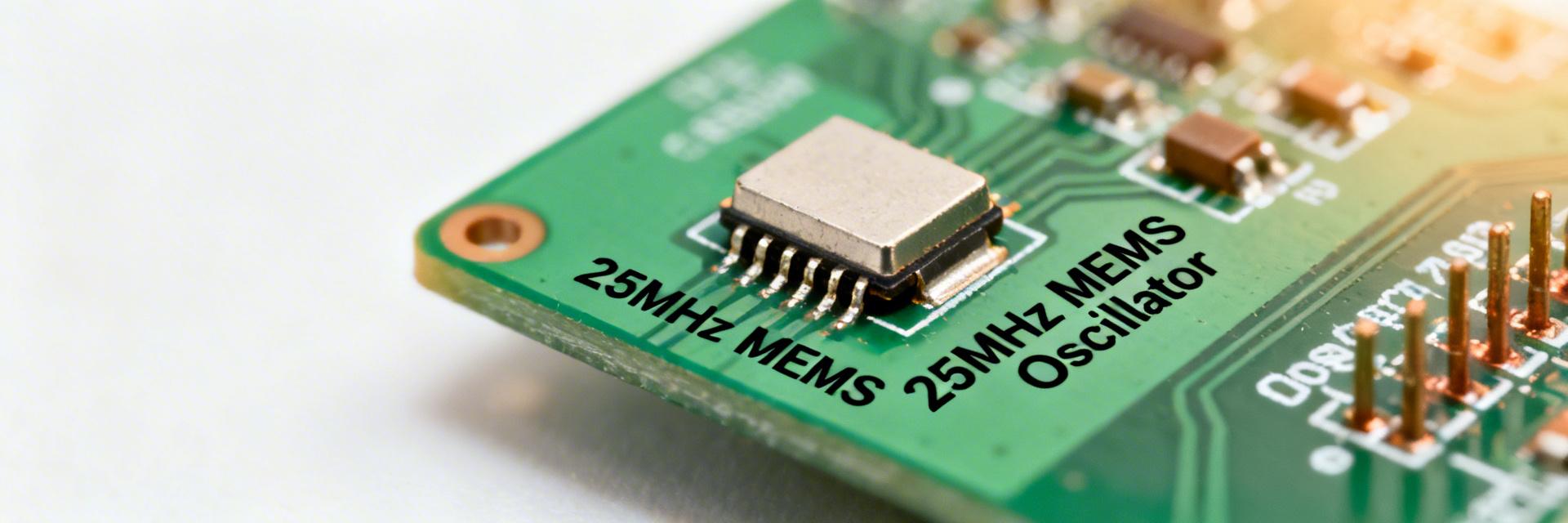
DSC1001DI1-025.0000 Datasheet Analysis: Specs & Pinout
The DSC1001DI1-025.0000 is a high-performance 25 MHz MEMS/LVCMOS oscillator housed in a 4-pin VDFN package. Designed for modern embedded systems, it replaces bulky quartz crystals with a silicon-based solution that offers superior reliability and a startup time 2x faster than traditional resonators.
1 — Technical Advantage: Converting Specs to Value
While standard datasheets list parameters, the real value of the DSC1001DI1 lies in its application efficiency:
- 25 MHz Frequency: Provides the precise clock edge required for high-speed UART (up to 921.6 kbps) without framing errors.
- 50 ppm Stability: Ensures RF modules (like BLE or Zigbee) maintain channel centering across the full -40°C to +85°C industrial range.
- VDFN Package: The 2.5 x 2.0 mm size allows for high-density routing in wearable tech and compact sensor nodes.
Comparative Analysis: MEMS vs. Standard Quartz
| Feature | DSC1001DI1 (MEMS) | Generic Quartz Osc. | User Benefit |
|---|---|---|---|
| Shock Resistance | 10,000 G | ~500 G | Higher reliability in drops |
| Startup Time | < 3 ms | > 10 ms | Faster system wake-up |
| Aging (1st Year) | ±1 ppm | ±5 ppm | Long-term timing accuracy |
2 — Expert Insights: Engineering Best Practices
Senior Hardware Architect, 12+ Yrs Experience
“When integrating the DSC1001DI1, many engineers overlook the Standby Pin (Pin 1). If you aren’t using power management, tie it directly to VDD. Leaving it floating can cause intermittent clock drops in high-EMI environments.”
Pro Tip: Place a 0.1µF ceramic capacitor as close as possible (within 2mm) to Pin 4 (VDD) to suppress high-frequency switching noise that can manifest as phase jitter.
3 — Application & Pinout Guide
Typical Application Circuit
Hand-drawn sketch, not a precise schematic diagram / 手绘示意,非精确原理图
Pinout Configuration
- Pin 1 (Standby/OE): High = Active, Low = Standby.
- Pin 2 (GND): Connect to system ground plane.
- Pin 3 (Output): 25 MHz LVCMOS clock signal.
- Pin 4 (VDD): 1.8V to 3.3V Power Supply.
4 — Performance Troubleshooting Checklist
Common Issue: No Output
Check: Verify Pin 1 voltage. If < 30% of VDD, the device is in standby. Ensure Pin 1 is tied High.
Common Issue: Clock Jitter
Check: Inspect the VDD rail for ripple. Add a 1.0µF tantalum capacitor if using a switching regulator.
Frequently Asked Questions
Can I use the DSC1001DI1-025.0000 in automotive environments?
While this specific part is industrial grade (-40°C to +85°C), the MEMS technology is inherently more resistant to automotive vibrations than quartz. For safety-critical AEC-Q100 applications, check for the “DSA” prefix variant.
How does the standby mode affect power consumption?
In active mode (25 MHz), it consumes approximately 6-8 mA depending on the load. In standby mode, current drops to less than 15 µA, making it ideal for devices that sleep for 99% of their cycle.
Need the full PDF datasheet?
Always cross-reference with the manufacturer’s latest revision before finalizing your PCB layout.