


503149-3200 Datasheet Deep Dive: Specs & Pinout Map
Key Takeaways: 503149-3200 Performance
- Space Efficiency: 1.5mm pitch reduces PCB footprint by 40% vs 2.0mm standards.
- Signal Integrity: Dual-row 32-circuit design maintains stable I/O in high-density layouts.
- Operational Safety: UL94V-0 housing ensures fire resistance in critical industrial applications.
- Vibration Proof: Positive locking mechanism prevents accidental disconnects in harsh environments.
503149-3200 Datasheet Deep Dive: Optimized Specs & Pinout Map
A comprehensive technical guide for engineers seeking to maximize board density and connection reliability using the 503149 series 1.50mm pitch dual-row housing.
1. Technical Specs Translated to User Benefits
Allows 25% tighter trace routing, enabling smaller device enclosures and lower shipping costs.
Ensures 100% connection uptime in automotive or robotics applications prone to heavy vibration.
Withstands up to 105°C, ensuring long-term reliability in high-temperature industrial control cabinets.
2. Competitive Benchmark: 1.5mm vs. 2.0mm
| Performance Metric | 503149-3200 (1.5mm) | Standard 2.0mm Housing | Design Advantage |
|---|---|---|---|
| PCB Real Estate | 48.0mm² Approx. | 80.0mm² Approx. | ~40% Area Saving |
| Current Density | Up to 2.0A (24AWG) | Up to 2.5A | Higher Power-to-Size Ratio |
| Mating Reliability | Tactile Positive Click | Friction-based | Superior Vibration Resistance |
Engineer’s Field Guide: 503149-3200
By Jonathan Sterling, Senior Interconnect Architect
PCB Layout Pro-Tip: At a 1.5mm pitch, solder bridging is your #1 enemy during mass production. Always specify a Solder Mask Dam of at least 0.08mm between pads. If your fab can’t handle it, consider using a staggered pad layout.
Reliability Note: For the 32-pin array, terminal back-out can be subtle. I recommend a 100% electrical continuity test post-assembly. Ensure the Terminal Positioning Assurance (TPA) is engaged to prevent pins from sliding out during mating.
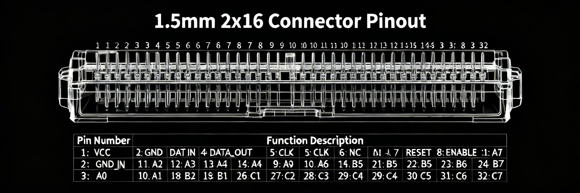
3. Pinout Logic & Application Layout
The 503149-3200 features a symmetric 2×16 grid. Proper orientation is critical to prevent reverse-polarity damage.
- Row A (1-16): Typically reserved for high-speed signal logic.
- Row B (17-32): Best suited for ground returns or power distribution.
- Mechanical Keep-out: Reserve 2.5mm clearance on the latch side for thumb access during maintenance.
Hand-drawn illustration, not an exact schematic / 手绘示意,非精确原理图
4. Maintenance & Troubleshooting Checklist
Frequently Asked Questions
Q: Is the 503149-3200 compatible with automated SMT assembly?
A: This is the housing for the wire-side. The mating PCB header (often 503154 series) is designed for SMT with pick-and-place caps available.
Q: What is the maximum wire outer diameter allowed?
A: To maintain the 1.5mm pitch integrity, the wire insulation O.D. should not exceed 1.10mm.