


FS32K144 MCU: Complete Spec & Pinout Benchmark Guide
Recent benchmark suites show 32-bit MCUs with hardware safety and on‑chip flash delivering roughly 20–35% improvement in body‑electronics throughput year‑over‑year. This guide frames why the FS32K144 is the premier choice for safety‑critical embedded designs, providing a technical breakdown for system engineers.
Performance Throughput Benchmark
Year-over-year improvement in body-electronics processing efficiency.
FS32K144 at a Glance — Key Specs & Architecture
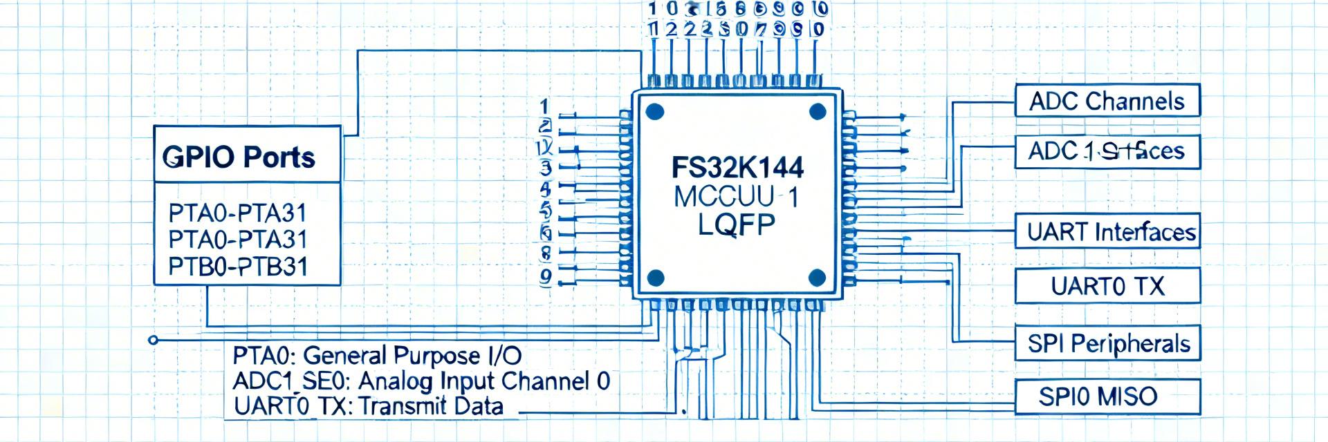
Architecture & Core Capabilities
The FS32K144 class targets 32‑bit, floating-point capable cores with clock domains sized for mid-range automotive and industrial workloads; typical core frequencies and boost modes yield measurable DMIPS scaled to system clocks. On‑chip flash and RAM sizes directly affect boot latency, logging throughput, and ISR jitter, making memory choices central to real tasks.
Safety, Security & Peripheral Overview
Built‑in safety primitives emulate ASIL-style mechanisms such as ECC, dual watchdog strategies, and lockstep checks; secure boot and crypto accelerators reduce runtime attack surface. Peripheral families cover timers, ADC/DAC, SPI/I2C/UART, and CAN/LIN‑like comms. These features define system partitioning between safety-critical paths and best-effort services.
Complete Technical Specification Breakdown
| Feature Category | Technical Specifications |
|---|---|
| CPU Performance | ARM Cortex-M4F, up to 112 MHz, Floating Point Unit (FPU) |
| Memory Tiers | 512 KB Flash (with ECC), 64 KB SRAM |
| Communication | 3x CAN (FD capable), 3x LPSPI, 3x LPUART, 2x LPI2C |
| Analog Units | 2x 12-bit ADC (up to 16 channels), 1x 8-bit DAC |
| Operating Voltage | 2.7V to 5.5V (Wide supply range for automotive stability) |
Memory, CPU Performance & Clock Domains
Expect flash options and RAM tiers to span small to mid sizes; cache behavior, bus matrix arbitration, and peripheral clock gating shape real throughput. Benchmark targets should include sustained flash read/write latency, DMA throughput, CPU DMIPS under mixed ISR load, and context‑switch latency under preemption to mirror ECU and fusion workloads.
Power, IO Ratings & Environmental Specs
Key power fields include VDD ranges, IO domain voltages, and multiple low‑power modes. Engineers must plan decoupling, absolute maximums, and EMC mitigation early. Typical current draw in active and sleep states, thermal derating and recommended decoupling networks are crucial spec items for robust field performance and emissions compliance.
Pinout & Package Options — Detailed Mapping
Pin Functions, Groups & Alternate Muxing
Pin grouping follows port conventions with multi‑function pins subject to alternate‑mux rules; reading package pin tables shows default and remapped assignments. Choose pins for high‑speed signals that minimize cross‑talk, reserve analog‑capable pins for ADC channels, and prefer DMA‑friendly pins for heavy peripheral traffic when mapping FS32K144 UART or sensor buses.
Package Footprints, Thermal & PCB Placement Tips
Common packages include QFN, LQFP, and denser BGA‑like options; pad layout and thermal via placement impact thermal dissipation and reflow yields. Split power/ground planes, place decoupling near power pins, and route high‑speed comms with controlled impedance. Consider thermal vias beneath exposed pads for sustained high‑power operation.
Benchmark Methodology: How to Test FS32K144 Specs & Pin Performance
System-level Setup
Define a testbench with clean clock sources, regulated rails, and a minimal reference board. Capture metrics like CPU DMIPS, flash latency, and ISR jitter using repeatable recipes and baseline fixtures.
Electrical SI Tests
Toggling pins across frequency sweeps reveals rise/fall, overshoot, and crosstalk. Specify pass/fail thresholds for ringback and jitter, collecting data with CSV fixtures for automated processing.
Practical Pin Mapping & Reference Patterns
-
•
Typical mappings: UART, CAN-like networks, ADC, PWM & sensors Recommended mappings prioritize signal integrity and DMA use: assign debug UART to isolated pins, map multi‑channel ADC to contiguous analog pins, and locate PWM outputs near power stages to limit return loop area.
-
•
PCB routing checklist & BOM-level considerations Place decoupling capacitors within millimeters of VDD pins, route ground returns with unbroken planes, and isolate high‑speed lanes. Add series resistors and ferrite beads near transceivers for production reliability.
Integration, Debugging & Production Readiness
Firmware Bring-up
Validate supply sequencing, clock trees, and secure boot vectors; enable basic peripherals incrementally. Systematic bring‑up reduces time to integration and simplifies root cause analysis.
Safety & Compliance
Compile a pre‑production checklist including boundary‑scan, in‑circuit tests, and safety diagnostics. Design production fixtures with deterministic test vectors for traceability.
Summary
- ✓ The FS32K144 family balances floating‑point compute, on‑chip flash, and safety primitives to accelerate body‑electronics and industrial throughput.
- ✓ Pinout choices drive signal integrity and DMA efficiency—map UART, CAN, ADC, and PWM with isolation and termination in mind.
- ✓ Apply repeatable benchmark recipes and follow the integration checklist for production readiness to shorten time‑to‑market.