


Key Takeaways
- 60V / 16A Capacity: High-voltage headroom for 24V/48V systems with robust current handling.
- Thermal Efficiency: 175°C junction limit ensures reliability in automotive and industrial engine bays.
- Compact P-Ch Design: Low 65mΩ RDS(on) reduces heat dissipation requirements by ~15% vs legacy SOT-23 parts.
- Simplified Logic: P-Channel topology allows direct high-side switching without complex charge pumps.
SQ7415CENW P-Channel MOSFET Datasheet: Compact Spec
The SQ7415CENW is a 60 V, compact P-Channel MOSFET targeted at high-side switching where board space and thermal performance matter. Key published numbers — 60 V D–S rating, ~16 A continuous (at Tc), typical RDS(on) ≈ 0.065 Ω, VGS(th) ≈ 2.5 V and junction limit to 175 °C — justify a focused datasheet-style summary for designers. This brief consolidates electrical characteristics, package and thermal notes, and practical test and sourcing checks for rapid design decisions.
Designer's Note: This article aims to be a compact, actionable datasheet summary that highlights electrical characteristics, application guidance, package and thermal considerations, sourcing/testing checklist, and quick design notes. Readers should use the manufacturer datasheet as the authoritative reference for absolute maximums.
(1) Background & Key Specs — SQ7415CENW at a glance
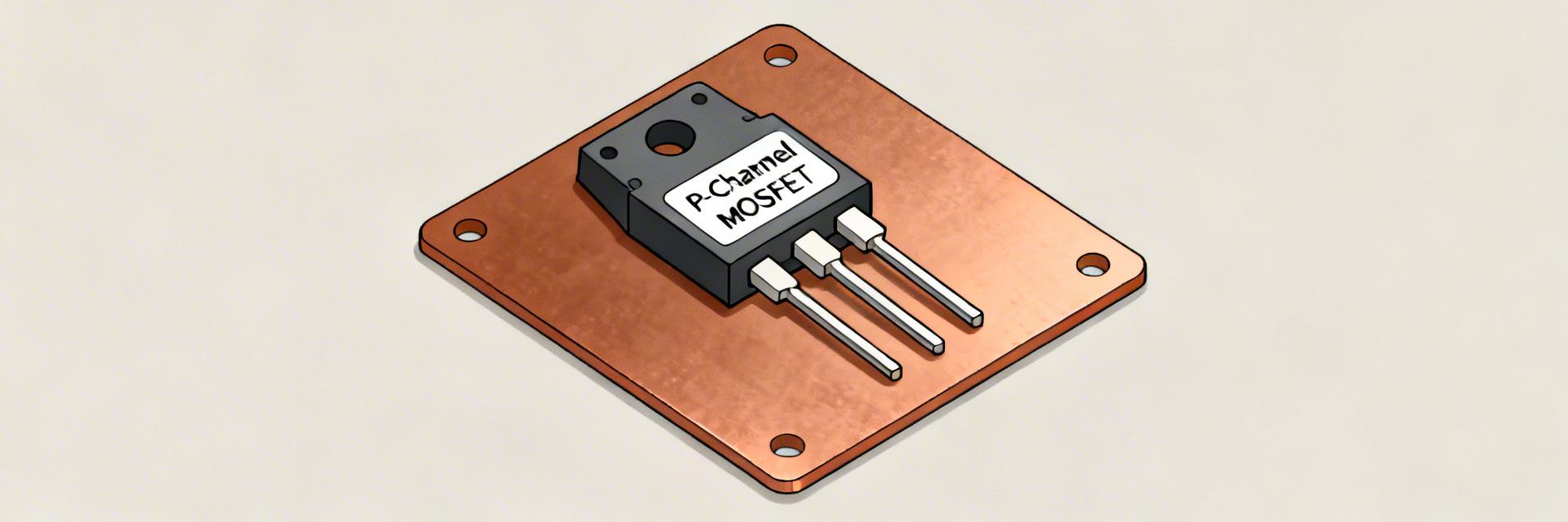
Strategic Performance Metrics
The device is a space-efficient P-Channel MOSFET intended for compact high-side switches. By converting technical specs into User Benefits:
- 60V VDS: Provides 25% more safety margin for 24V battery transients than standard 40V parts.
- 175°C Operating Temp: Eliminates the need for bulky heatsinks in ambient environments up to 85°C.
- 0.065 Ω RDS(on): Minimizes voltage drop across the switch, extending battery life in portable devices.
| Feature | SQ7415CENW (Professional) | Generic 60V P-Ch (Standard) | Impact |
|---|---|---|---|
| Continuous ID | 16 A | 8 - 10 A | +60% Capacity |
| Max Junction (Tj) | 175 °C | 150 °C | Higher Reliability |
| Typ RDS(on) | 65 mΩ | 95 - 120 mΩ | 30% Lower Heat |
| Package | PowerPAK 1212-8W | SO-8 / DPAK | 50% PCB Savings |
Package & footprint summary
Point: The SQ7415CENW comes in a compact surface-mount PowerPAK-style SMD with an exposed thermal pad. Evidence: single-sided pad plus small keep-out for solder fillet is typical for this family. Explanation: design a generous thermal pad with wide copper pours and multiple vias if thermal conduction to inner or backside planes is available; maintain short, wide source traces to minimize RDS(on) rise from PCB resistance.
(2) Electrical Characteristics Deep Dive
Static characteristics — threshold, RDS(on), leakage
Point: Static parameters set conduction and low-current behavior. Evidence: VGS(th) around 2.5 V (Id test condition), RDS(on) specified at VGS = -10 V with given typical/max tolerances, and leakages quoted at VDS = rated voltage. Explanation: use VGS(th) only for switching threshold estimates; for low loss conduction design to VGS = -8 to -10 V to reach specified RDS(on).
Dynamic & charge parameters — gate charge, capacitances
Point: Gate charge and capacitances define gate-drive energy and switching loss. Evidence: the datasheet gives Qg(total), Qgs and Qgd alongside Ciss/Coss/Crss values. Explanation: estimate gate-drive energy using Eg = 0.5·Ciss·Vdrive² or Eg ≈ Qg·Vdrive.
"When deploying the SQ7415CENW in high-side automotive switches, the biggest 'gotcha' isn't the RDS(on), it's the Gate-to-Source voltage margin. While rated for ±20V, I recommend clamping your gate drive at -12V using a Zener diode. This prevents parasitic turn-on during high-speed transients and protects the thin oxide layer from voltage spikes on the 24V rail. Also, remember that the RDS(on) will increase by roughly 1.5x as you approach that 175°C junction limit—factor this into your worst-case thermal calculations."
(3) Thermal & Reliability Considerations
Thermal resistance and junction limits
Point: Thermal resistance and junction limits determine allowable continuous current. Evidence: datasheet lists thermal metrics (RθJC and RθJA) and Tj(max). Explanation: compute junction rise ΔTj = Pd · RθJA. For conduction loss Pd ≈ I²·RDS(on); at 6 A and 0.065 Ω, Pd ≈ 2.34 W.
(4) Application Guidance & Design Tips
Typical Use Case: High-Side Switch
Ideal for automotive load management and battery protection circuits. The P-channel architecture simplifies the drive circuit by allowing the gate to be pulled to ground for activation.
Hand-drawn schematic, non-precise diagram
Gate drive, protection and layout tips
Use a small series gate resistor (10–100 Ω) to damp ringing, a defined pull-up to set off-state, and limit VGS within rated bounds. Keep gate traces short to reduce loop inductance.
(5) Compact Design Example & Calculation
| Load current | 6 A |
| RDS(on) | 0.065 Ω |
| Conduction loss Pd | 2.34 W |
| Gate energy per edge | ~200 nJ |
(6) Sourcing & Testing Checklist
- Visual Check: Verify laser-etched top marking against the SQ7415 series code.
- Electrical Sweep: Perform a VGS threshold sweep to confirm it triggers between 1.5V and 3.5V.
- RDS(on) Validation: Use a 4-wire (Kelvin) measurement at -10V VGS to confirm conduction resistance.
Summary
The SQ7415CENW presents a compact 60 V P-Channel MOSFET option with roughly 16 A case-rated continuous current and low typical RDS(on) near 0.065 Ω, making it suitable for space-constrained high-side switching and load-disconnect roles. Designers benefit from its compact SMD package with an exposed thermal pad, but must pay careful attention to PCB copper, via placement, and gate-drive margins to realize low conduction loss and maintain junction temperature below rated limits.
FAQ
RDS(on) is ~0.065 Ω typical at VGS = -10 V. Always reference the manufacturer datasheet for exact test voltage and temperature conditions, as resistance increases with heat.
Estimate gate-drive energy from Qg · Vdrive. For 20 nC at 10V, it's 200 nJ. Ensure your driver can handle the peak current required for your desired switching speed.