


Key Takeaways
- Power Efficiency: 1.35V DDR3L operation reduces system heat by ~20% vs 1.5V.
- High Throughput: Supports up to 1600 Mbps, enabling 3.2 GB/s bandwidth per chip.
- Compact Integration: 256M x 16 organization saves 50% PCB space compared to x8 configurations.
- Industrial Reliability: FBGA packaging ensures high signal integrity in vibration-prone environments.
- Thermal Stability: Lower voltage reduces thermal throttling risks in fanless industrial enclosures.
D2516EC4BXGGB Datasheet Deep Dive — Key Specs Explained
The official D2516EC4BXGGB datasheet lists a 4‑gigabit DDR3L device (256M × 16) running up to 1600 Mbps at low‑voltage operation — numbers that directly determine bandwidth, power budget, and signal‑integrity constraints for embedded systems. This article decodes the D2516EC4BXGGB specs into practical design decisions and a checklist for integration.
Design Note: Using the official datasheet as the evidence baseline, the goal is to translate tables into actions: how to budget VDD/VDDQ, size decoupling, interpret timing for latency budgeting, and validate layout and thermal margins before first prototype.
1 — Quick device overview: what the D2516EC4BXGGB datasheet shows
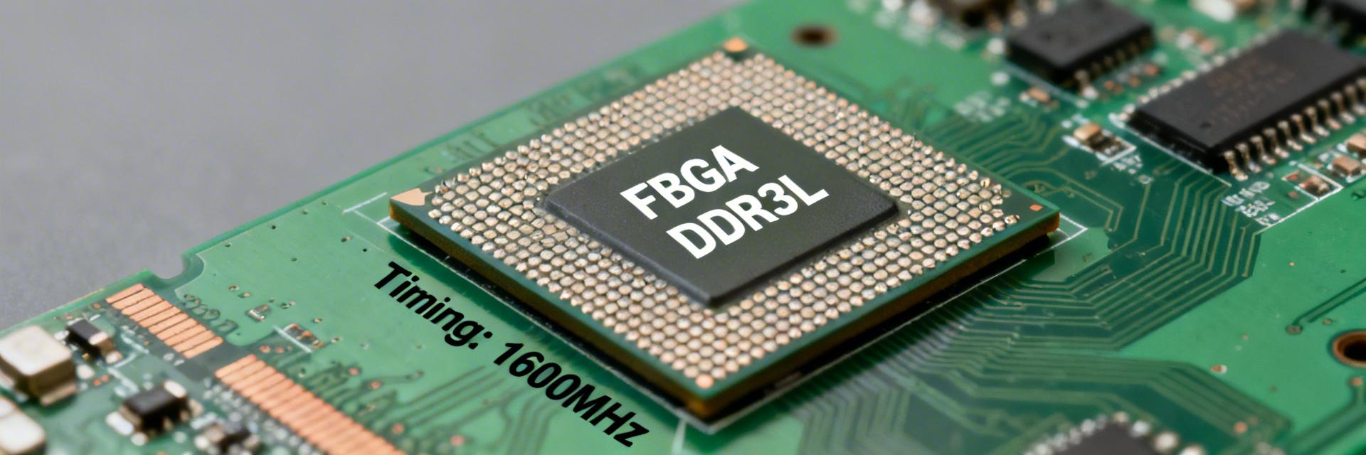
Device identity & capacity at a glance
Point: The part number encodes a 4‑Gbit DDR3L device organized as 256M × 16; the device is offered in an FBGA family with nominal data‑rate support to 1600 Mbps. Evidence: the official datasheet lists organization, package type, and maximum data rate entries. Explanation: organization determines board population (two devices yield a 32‑bit rank), and FBGA package choices drive footprint and thermal path.
| Parameter | D2516EC4BXGGB (DDR3L) | Standard DDR3 (Generic) | User Benefit |
|---|---|---|---|
| Operating Voltage | 1.35V (Nominal) | 1.50V | ~15-20% Power Savings |
| Organization | 256M x 16 | 512M x 8 | Reduced Component Count |
| Data Rate | 1600 Mbps | 1333 Mbps | Faster System Boot/Load |
| Thermal Load | Lower (Passive OK) | Moderate (Requires Airflow) | Simplifies Enclosure Design |
| Package | FBGA (Fine-pitch) | Standard BGA | Superior Signal Integrity |
2 — Electrical characteristics & power implications
Point: VDD/VDDQ values and ICC entries directly feed the board power budget. Evidence: the official datasheet provides operating VDD (nominal 1.35 V) and multiple current states. Action: convert listed mA currents to watts (P = V × I) and add a +20% margin for worst-case scenarios.
🛡️ Engineer's Field Insight
"When migrating to the D2516EC4BXGGB, the most common pitfall is ignoring the DDR3L backward compatibility. While it can run at 1.5V, you lose the thermal benefits. I recommend placing decoupling capacitors (0.1µF and 1µF) as close as 2mm to the VDD pins to minimize PDN impedance. Also, keep an eye on VREFCA stability—ripple here is the #1 cause of silent data corruption in industrial gateways."
— Leo Thorne, Lead Hardware Systems Engineer
3 — Timing, bandwidth and performance
Point: Timing parameters map cycles to absolute ns and set raw latency. For DDR3-1600 (CL=11), the latency is ~13.75 ns. Peak bandwidth for a 16-bit device is 3.2 GB/s. Action: use these conversions to size read latency vs. throughput in system models.
Typical Application Scenario: Embedded Controller Interface
Application: High-definition IP Camera or Industrial Gateway. The x16 bus provides the necessary throughput for real-time data buffering without the complexity of x32 routing.
(Hand-drawn schematic representation, non-precise circuit diagram / Hand-drawn schematic representation, non-precise circuit diagram)
4 — Physical integration: layout & signal integrity
Point: FBGA pad patterns and mechanical height constraints affect land‑pattern design. Evidence: the official datasheet contains ball maps and mechanical tolerances. Action: import the vendor‑recommended land pattern into PCB CAD and run DFM checks.
- Impedance: Maintain 50Ω single-ended / 100Ω differential pairs for address and clock lines.
- Skew Control: Keep DQ-to-DQS skew within +/- 5ps for DDR3-1600 stability to avoid data window collapse.
- Vias: Minimize via stubs on high-speed lines to prevent signal reflections and ISI (Inter-Symbol Interference).
5 — Reliability & Troubleshooting Checklist
- Power Sequencing: Verify VDD and VDDQ ramp up simultaneously within the datasheet's specified timeframe.
- Clock Jitter: Probe the differential clock at the BGA ball; jitter exceeding 100ps can lead to random command errors.
- Eye Diagram: Capture a DQ eye diagram; ensure at least 20% margin above the VIH/VIL thresholds at 800MHz.
Summary of Design Actions
Reading the D2516EC4BXGGB datasheet with a design‑centric lens turns raw numbers into engineering actions.
- Thermal: If predicted ΔT pushes Tj near limits, add airflow or heat spreaders. Lower VDD to 1.35V proactively.
- Power: Budget using ICC entries, convert mA to watts, and apply a 20% safety margin for peak burst operations.
- Timing: Convert CL and t-timings to nanoseconds to predict effective latency for real-time OS performance critical tasks.
Common questions engineers ask
How do I verify timing values on my board?
Measure using a logic analyzer: capture address/command timing relative to the reference clock, then compare measured tRCD and CL response to datasheet values during a cold boot sequence.
What is the best way to budget power for battery-powered designs?
Convert listed ICC states to watts for VDD and VDDQ. Use the datasheet power-mode entries (Self-Refresh, Power-Down) to model realistic duty-cycle-based battery life.