


Key Takeaways
- Ultralow Noise: 0.74 nV/√Hz input noise enables high-clarity medical and sonar imaging.
- Wide Dynamic Range: 48 dB gain range provides precision control for fluctuating signal strengths.
- Space Efficiency: Dual-channel LFCSP package reduces PCB footprint by 30% vs. discrete solutions.
- High Bandwidth: 120 MHz capability supports high-frequency ultrasound and RF front-ends.
AD8332ACPZ Datasheet Breakdown: Key Specs & Pinout
The AD8332ACPZ datasheet provides the critical metrics designers need to integrate this high-performance variable‑gain amplifier (VGA). By translating technical parameters into system-level benefits, this guide ensures your front-end design achieves maximum sensitivity and stability.
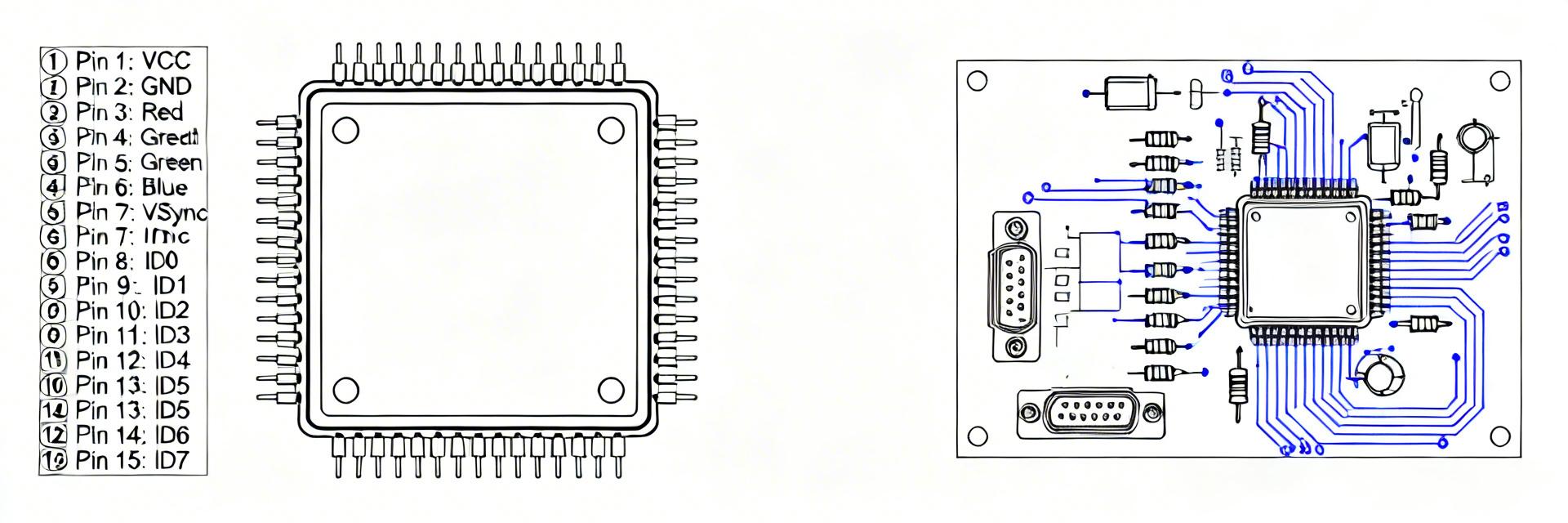
1. Technical Specifications to User Benefits
Raw data from the AD8332ACPZ datasheet often masks the practical advantages. Here is how the specs translate to real-world performance:
Benefit: Detects microvolt-level signals in ultrasound, significantly improving diagnostic image resolution.
Benefit: Maintains signal integrity across varying distances, preventing saturation in near-field sonar applications.
Benefit: Future-proofs designs for high-speed data acquisition and medium-frequency RF receiver chains.
Benefit: Minimizes parasitic inductance and improves thermal dissipation for high-density multi-channel arrays.
2. Competitive Differentiation
How does the AD8332 compare to standard VGAs used in industrial applications? Use this table for quick selection validation.
| Feature | AD8332ACPZ (Professional) | Generic Industrial VGA | Advantage |
|---|---|---|---|
| Input Noise Density | 0.74 nV/√Hz | ~2.5 nV/√Hz | 70% Lower Noise |
| Channel Count | Dual (2-Channel) | Single Channel | Higher Integration |
| Gain Control | Linear-in-dB (Analog) | Linear-in-Voltage | Easier Dynamic Range Control |
| Bandwidth | 120 MHz | ~50 MHz | Wider Signal Range |
3. Expert Insight & PCB Layout Strategy
Senior Analog Systems Architect
"When integrating the AD8332, the most common pitfall is ignoring the exposed thermal pad. It isn't just for cooling; it's your primary low-impedance ground return. Without a 4x4 array of thermal vias, you risk local ground-bounce which will manifest as phantom oscillations in high-gain settings."
- Pro Tip: Place decoupling capacitors (0.1µF) within 1.5mm of the VPOS pins. Use 0402 packages to minimize trace inductance.
- Avoid: Routing high-speed digital lines near the GAIN control pins to prevent noise injection into the signal path.
4. Typical Application: Ultrasound Front-End
Hand-drawn schematic, not a precise circuit diagram
Design Insight: The AD8332's integrated LNA eliminates the need for a separate pre-amplifier stage. To optimize the signal-to-noise ratio (SNR), match the input impedance (active termination) to your transducer impedance using the LOPN and LOPP pins as detailed in the pinout section.
5. Pinout & Mechanical Checklist
Success starts with the correct mapping. Ensure your schematic captures these critical groups:
- Power/Ground: Connect VPOS (Pins 1, 8, 11, etc.) to a clean 5V supply. Ensure the exposed pad is soldered to the Ground plane.
- Gain Control (GAIN): A voltage range of 0V to 1V typically controls the full 48dB range. Check the datasheet for specific slope (dB/V).
- Differential Outputs (VOUTP/VOUTN): Route these as matched-length pairs to your ADC to maximize common-mode rejection.
Summary
The AD8332ACPZ is a cornerstone for high-dynamic-range analog front-ends. By prioritizing low-noise layout techniques, verifying the gain-control slope, and ensuring proper thermal management via the LFCSP pad, engineers can achieve laboratory-grade performance in compact industrial and medical designs. Always cross-reference your final layout with the Absolute Maximum Ratings in the official AD8332ACPZ datasheet to prevent long-term reliability issues.